Materials Science Laboratory
Light-emitting transistors (LETs), which are based on
high-speed heterojunction bipolar transistors (HBTs) with a quantum well
(QW) in the base layer, are electrical devices as well as optical ones
[1]. According to the principles of their operation, LETs can run faster
than conventional light-emitting diodes (LEDs). Since nitride-based semiconductor
LEDs are commercially available for lighting, it is expected that the nitride-based
semiconductor LETs will work as light sources for visible light communication
[2]. In this work, we fabricated nitride-based semiconductor LETs and investigated
their optical output characteristics.
We fabricated pnp AlGaN/InGaN/GaN LETs with a 3-nm-thick
QW in the base layer. The In mole fraction of the InGaN QW was higher than
that of the InGaN base layer. When we apply forward bias at the emitter-base
junction of the LETs, holes are injected from the emitter to the base layer.
The injected holes diffuse toward the collector and are captured at the
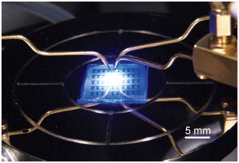
QW. Some of the uncaptured holes reach the collector. Figure 1 shows a
photograph of the emission from the LETs under forward bias conditions.
We can observe the strong purplish emission with the peak wavelength of
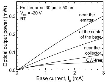
410 nm. Next, we fabricated three types of LETs with the QW position varied
in the base layer: near the emitter, at the center of the base, and near
the collector. Figure 2 shows the optical output power as a function of
the base current for the three LETs. We also show the output power for
a QW-free LET (standard HBT) as a reference. The output power with the
QW near the collector is weaker than with it near the emitter. This indicates
that the probability of the hole capture depends on the position of the
QW. The velocity of the holes diffusing in the base becomes larger as the
holes approach the collector, which results in a lower hole capture probability
near the collector. We achieved 0.3-mW optical output power from the LET
with the QW near the emitter at the base current of 0.3 mA, corresponding
to the external quantum efficiency of 3.3 %. We will investigate the electrical
and optical modulation properties of the LETs for high-speed operation,
which may open an avenue to their application as high-speed visible light
sources.
[1] M. Feng et al., Appl. Phys. Lett. 84 (2004) 1952.
[2] Y. Tanaka et al., IEICE Trans. Commun. E86-B (2003) 2440.
[3] K. Kumakura et al., Int. Conf. Solid State Devices and Materials, 2011 Nagoya, A-4-2.
 |
 |
|||||
|
|