Materials Science Laboratory
Graphene, a two-dimensional (2D) crystalline sheet of carbon,
has generated considerable attention owing to its ultrathin geometry and
high carrier mobility, with potential application in high-performance low-power
electronics. It has been shown that the band gap of graphene can be controlled
when it is tailored into a ribbon shape with a width of up to several nanometers
[1]. However, methods such as lithography do not satisfy the requirements
for the ideal nanoribbons in terms of production efficiency, uniformity
of crystal orientation, and edge structure. On the other hand, it has been
reported that a buffer layer on a SiC(0001) surface is decoupled from the
substrate by H intercalation and it turns into graphene (quasi-free-standing
monolayer graphene, QFMLG) [2]. Although the buffer layer is a 2D sheet
of carbon like graphene, it is electrically insulating due to covalent
bonds with the substrate. It is desirable to desorb H atoms partially and
create insulating regions in QFMLG for fabrication of graphene nanostructures.
We investigated H desorption from QFMLG and found a self-organization of
QFMLG nanoribbon networks during the H desorption process.
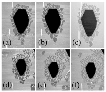
We performed in-situ STM observations of the H desorption
process on QFMLG. Above 630°C, H-desorbed regions expand from SiC step edges (Fig. 1). Each H-desorbed
region increases in size and is split into several patches by QFMLG nanoribbons.
Finally, H-desorbed patches separated by the network of QFMLG nanoribbons
cover the entire surface. The average width and length of the QFMLG naoribbons
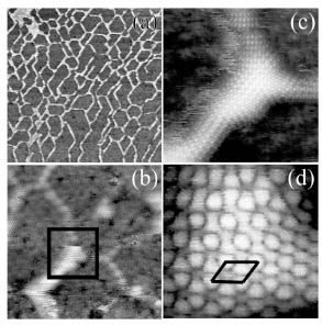
are a few nanometers and ~10 nm, respectively. The nanoribbons run along the SiC[11![]() ×
×![]() surface structure, indicating electron scattering at the boundary between
the QFMLG and H-desorbed regions (Fig. 2) [3].
surface structure, indicating electron scattering at the boundary between
the QFMLG and H-desorbed regions (Fig. 2) [3].
[1] M. Y. Han et al., Phys. Rev. Lett. 98 (2007) 206805.
[2] C. Riedl et al., Phys. Rev. Lett. 103 (2009) 246804.
[3] K. Sakai., Phys. Rev. B 81 (2010) 235417.
 |
 |
|||||
|
|