Physical Science Laboratory
Down scaling of semiconductor devices has been providing us
the opportunity to explore a new approach to devices with a limited amount
of dopants in the active device area, whose functionality is based on individual
dopants. Recent progress in nanofabrication has led to the observation
of the charge of a single dopant in silicon nanotransistors [1] and the
operation of a single-atom electron spin qubit in silicon [2].
Recently we have investigated a novel device concept
based on single dopant functionality, that is, we have demonstrated multiple-donor
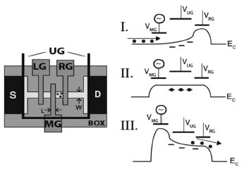
based single electron pumps [3]. Our devices consist of Si nanowire MOSFETs
in series fabricated on a silicon-on-insulator (SOI) wafer (see Fig. 1).
A stacked gate layer structure is employed; the lower layer consists of
three fine gates, LG (not used), MG, and RG, defined by electron beam lithography,
and the top layer consists of a large single upper gate (UG). Donor atoms
(arsenic) are locally implanted in the nanowire channel between MG and
RG using a 60 nm wide aperture in a resist mask. For charge transfer operation
(see Fig. 1 right), we apply an AC signal with a frequency f to MG. RG is tuned such that it induces a small barrier in the Si nanowire beneath it. When the barrier formed by VMG is in its low state (I), electrons enter from the source. When the barrier
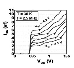
is subsequently ramped up (II) to its high state (III) by VMG, electrons are captured at donor sites, and then the gate electric field ionizes the donors and evacuates their bound electrons to the drain region. Figure 2 shows the charge pump characteristics ISD versus VUG at various right fine gate voltages (VRG). Current plateaus due to single-electron transfer via multiple dopants
are clearly observed. It is also shown that the number of dopants is tunable
by VRG; positively increased VRG reduces a depletion region in the island, making more donors available for charge transfer. Temperature-dependent characterization allows us to extract the ionization energy of a single arsenic donor. Dopant based SE pumps are capable of pumping multiple electrons with the number of dopants and therefore promising for electrical standards generating high currents.
[1] Y. Ono et al., Appl. Phys. Lett. 90 (2007) 102106.
[2] J. J. Pla et al., Nature 489 (2012) 541.
[3] G. P. Lansbergen, Y. Ono, and A. Fujiwara, Nano Lett. 12 (2012) 763.
 |
 |
|||||
|
|