Measurements
Koji Muraki, and Toshimasa Fujisawa*
Physical Science Laboratory, *Tokyo Institute of Technology
Plasmons, which are collective charge oscillations, could
provide a means of confining electromagnetic field to nanoscale regions.
Recently, plasmonics in graphene have attracted interest, particularly
because of the tunable plasmon dispersion. In this work, we carried out
time-resolved electrical measurements of edge magnetoplasmons (EMPs), which
are plasmons localized at graphene edge in a high magnetic field, and demonstrate
that the velocity of EMPs can be controlled over two orders of magnitude
[1].
Graphene used was grown on SiC substrate. We used two
samples, one with and the other without a large top gate. All measurements
were carried out at 1.5 K. Plasmons are injected into graphene by applying
a voltage step to the injection gate and detected through the detector
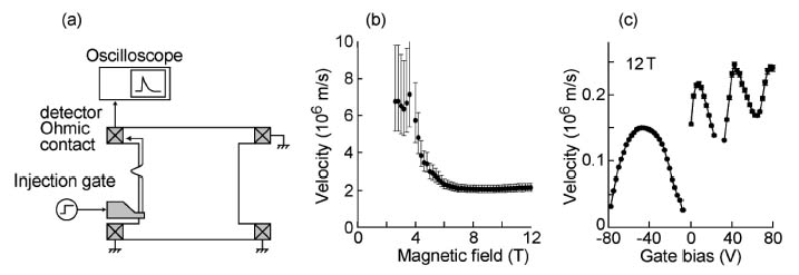
Ohmic contact fabricated 1.1 mm away from the injection gate [Fig. 1(a)].
From the time of flight between the injector and the detector, the plasmon
velocity is determined. In the ungated sample, as the magnetic field is
increased, the velocity decreases from 6000 km/s to 2000 km/s [Fig. 1(b)].
In the gated sample, on the other hand, the velocity is about 100 km/s,
which is one order of magnitude smaller than that in the ungated sample
[Fig. 1(c)]. The smaller velocity is due to the gate screening effect of
the electric field in plasmons. At a fixed magnetic field (12 T), as the
gate bias and thus the carrier density are decreased, the velocity decreases
to 10 km/s with oscillations. These results indicate that the velocity
of plasmons in graphene can be controlled over two orders of magnitude
by applying the magnetic field, screening the plasmon electric field with
a gate metal, and changing the carrier density. The wide tunability of
the plasmon velocity encourages designing graphene nanostructures for plasmonic
circuits.
This work was supported by KAKENHI.
[1] N. Kumada et al., Nature Commun. 4 (2013) 1363.
 |
||
|