Single-Crystal Cubic Boron Nitride Thin Film Growthby Ion-Beam-Assisted Molecular Beam Epitaxy
Cubic boron nitride (c-BN) with sp3-bonding has a large bandgap energy of 6.25 eV and a high breakdown field of ~ 8 MV/cm, which may further expand the potential of nitride-based semiconductor devices. However, conventional growth methods for group-III nitrides, such as MOVPE, have been unsuccessful in the growth of single-crystal c-BN films because c-BN is a metastable phase at ambient atmosphere. Here we report the epitaxial growth of single-crystal c-BN films by the ion-beam-assisted molecular beam epitaxy (MBE) method. We show that a proper adjustment of acceleration voltage for N2+ and Ar+ ions is the key to the selective formation of the c-BN phase.
BN thin films were grown on diamond(001) substrates by electron-beam evaporation of B in a flux of N2+ and Ar+ ions. The acceleration voltage (Vacc) for the ions was varied in the range from 200 to 450 V. The growth temperature (Tg) was varied in the range from 400 to 820oC. The supplied nitrogen/boron ratio was set at values > 1.
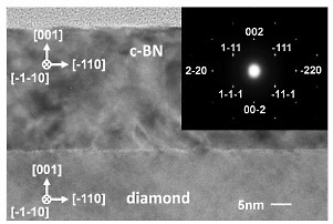
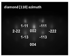
Single-crystal c-BN(001) films were obtained at Tg ≥ 750oC with Vacc = 280 V. The formation of the single-crystal c-BN was confirmed by cross-sectional TEM, selective area electron diffraction (SAED) and RHEED (Figs. 1 and 2) [1]. Although the designated thickness of the c-BN film was 160 nm, the resultant c-BN films were about 30-nm thick. This means
that ~ 80 % of supplied B atoms were etched by ion bombardments during the c-BN growth.
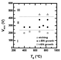
To obtain a clue to the growth mechanism of c-BN in the ion-beam-assisted MBE processes, we also carried out regrowth of BN films on single-crystal c-BN thin film templates on diamond substrates with the growth parameters systematically varied. A summary of those results provided us a phase diagram of BN, which was plotted as a function of Vacc and Tg
(Fig. 3). The phase diagram indicates a strong dependence on Vacc with much less dependence on Tg. At Vacc < 220 V (Region I), sp2-bonded turbostratic BN (t-BN) is predominantly formed. At Vacc between 220 and 450 V (Region II), single-crystal c-BN continues to grow. At Vacc > 450 V (Region III), the c-BN template is etched out as evidenced by an instantaneous change of the RHEED pattern back to that of the diamond(001) substrate. In short, at low acceleration voltages, sp2-bonded BN is dominantly formed, while at high acceleration voltages, etching dominates, irrespective of the bonding characteristics of BN. Consequently, the formation and epitaxial growth of metastable c-BN are achieved as a result of the interplay between competitive phase formation and selective etching [1].
This work was supported by KAKENHI.
- [1]
- K. Hirama et al., Appl. Phys. Lett. 104 (2014) 092113.
 |
 |
 |
|
|
|