Realizing Topological Insulating Phase in the Heterostructure Composed of Direct Transition Band Gap Semiconductors
Kyoichi Suzuki, Yuichi Harada, Koji Onomitsu*, and Koji Muraki
Physical Science Laboratory, *Material Science Laboratory
Topological insulators (TIs) have received substantial attention as a new state of matter, which cannot be classified into traditional materials such as metals, insulators, semiconductors, etc. TIs are characterized by distinct surface channels for three-dimensional (3D) TIs or distinct edge channels for two-dimensional (2D) TI composed of counterpropagating electron flows with opposite spin directions. In the channels, back scattering with spin reversal is prohibited. Therefore, TIs are promising for spintronic devices and low-power consumption devices.
In contrast with TIs confirmed so far, which have a conduction-valence band inversion in the material itself, we have succeeded in realizing a topological insulating phase arising from the heterojunction between InAs and GaSb, which both are III-V semiconductors with direct transition band gap [1]. Taking advantage of industrially developed semiconductor technologies, device application of TIs will be promoted. In addition, in the wake of our success, various combinations of materials will be investigated toward the development of new TIs.
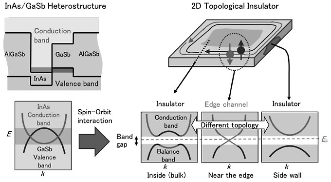
Figure 1 shows the schematic diagram of 2D-TI in the InAs/GaSb heterostructure. At the heterointerface, the conduction band bottom of InAs is lower in energy than the valence band top of GaSb as if conventional TI materials. By spin-orbit interaction, 2D-TI band structure is generated.
- [1]
- K. Suzuki, Y. Harada, K. Onomitsu, and K. Muraki, Phys. Rev. B 87 (2013) 235311.
|
- Fig. 1.
- Schematic diagram of 2D-TI generated from the InAs/GaSb heterostructure.
|
|
<< Prev | Contents | Next >>