AC Admittance of DNTT-Based MIS Capacitors
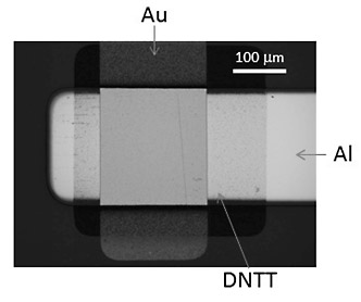
Frequency-dependent carrier dynamics in dinaphtho[2,3-b:2’,3’-f]thieno[3,2-b]thiophene (DNTT)-based metal-insulator-semiconductor (MIS capacitor) were studied by using admittance measurements [1]. The device structure is Al (50 nm) /AlOx (4 nm) /DNTT (30 nm) /Au (90 nm). Figure 1 shows an optical microscope
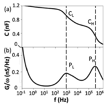
image of the sample. AC admittance Y (= G + jωC) was measured using a Solatron Impedance Analyzer. A small AC voltage VAC (=30 mV) superimposed on a DC voltage VDC was applied between the bottom gate and the top contact. Figure 2 shows the frequency dependence of the imaginary and real parts of the admittance divided by ω measured at VDC = –2.5 V. As the data show, the frequency dependences of C and G/ω are mutually correlated with each other. Two steps corresponding to the peaks in G/ω can be seen in C.
On the basis of an experimental study of devices with different contact geometries, peaks observed in the conductance spectra corresponding to slopes in the capacitance spectra were classified into two groups. The high-frequency peak PH was proportional to the top contact size and attributed to the carrier injection from the top contact to the DNTT/insulator interface just underneath the contact while the low-frequency peak PL was only observed when the device had DNTT region that was not covered by the top contact. The low-frequency peak was attributed to the drift current from the covered DNTT to the uncovered DNTT. The model calculation of carrier diffusion reproduces the low-frequency peaks very well. It is shown that the field-effect mobility from the accumulation region (–2.5 V) to the subthreshold region
(–1.1 V) can be estimated by fitting the data for each VDC.
- [1]
- T. Hayashi, N. Take, H. Tamura, T. Sekitani, and T. Someya, J. Appl. Phys. 115 (2014) 093702.
 |
 |
|
|