Growth of InP Nanowires on Graphene-Covered Fe
Recently, the large-scale growth of single-layer and few-layer graphene has been demonstrated by the roll-to-roll fabrication method, and the advanced technique of transferring graphene sheets to flexible plastic substrates has led to stretchable, foldable, and transparent electronics and optoelectronics [1]. Graphene layers can be formed on many kinds of substrates. Here, we report on InP nanowires (NWs) on graphene/SiC(0001) and graphene-covered Fe. The vapor-liquid-solid (VLS) method is widely used to make freestanding NWs. The growth is driven catalytically in a nano-area by nanometer-scale metal particles. This feature is very useful for fabricating nanodevices because of the feasibility of forming p-n junctions and various heterostructures like quantum dots and core-shell structures.
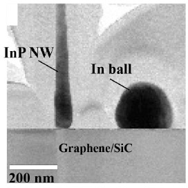
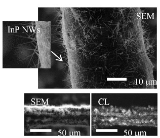
The VLS growth was carried out in a low-pressure metalorganic vapor phase epitaxy (MOVPE) reactor [2]. Trimethyl indium (TMIn) was the group-III source, and tertiarybutylphosphine (TBP) was the group-V source. We used Au particles as catalysts. The structures were observed by scanning electron microscopy (SEM) and transmission electron microscopy (TEM). III-V NWs tend to grow in the [111]B direction. Figure 1 shows a InP NW and an In ball grown on graphene/SiC(0001). Vertical NWs indicate that the (111)B face was likely to form initially on the 2D graphene surface. However, the low decomposition rate of TBP caused some In balls on the graphene surface. Some Au particles where the phosphorous supply was not enough could not form crystalline InP. This is due to less active sites on graphene to decompose TBP and also weak bonding characteristics of graphene surface. We have also tried to grow InP NWs on graphene/metal for flexible device application. After searching for proper metal among Cu, Ni and Fe, we could grow the NWs only on graphene/Fe. For Cu and Ni, the phosphorous reaction was so strong that it changed the surface morphology, which made the NW growth impossible. Fe forms various alloy compounds with carbon, and by adding carbon, Fe becomes harder, which is known as steel. The formation of steel would be important for the success of the subsequent InP NW growth. Figure 2 shows the demonstrated InP NWs grown on a micron Fe wire like spines of cacti. We also confirmed the cathodoluminescence (CL) from InP NWs. This system is very promising for a future NW application using flexible substrates.
- [1]
- S. Bae et al., Nature Nanotech. 5 (2010) 574.
- [2]
- K. Tateno et al., Jpn. J. Appl. Phys. 53 (2014) 015504.
 |
 |
|
|