InGaAs Photodetectors Based on Photonic Crystal Waveguide Including Ultrasmall Buried Heterostructure
Low-power optical link between CMOS chips and photonic network on chip have been extensively studied. One of the challenges with photodetectors (PDs) is to realize a small junction capacitance to use as a receiver in such short-range optical links. If the capacitance can be greatly reduced by reducing the size of the PDs, the RC constant could be kept at a low level even during connection with a high load resistor. The result would be a low thermal noise and an enhanced output voltage while maintaining a fast response. This would lead to the reduction of electrical amplification or even its elimination (referred as a receiver-less PD). There would then be a strong demand for nano-PDs with a small junction capacitance and high absorption efficiency.
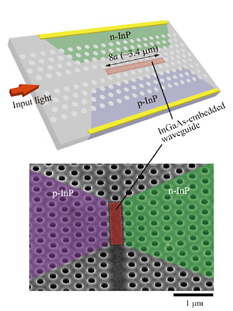
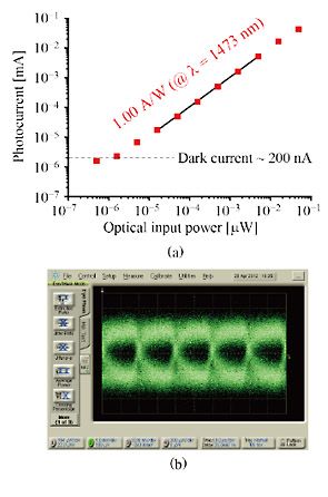
Semiconductor photonic crystal (PhC) can confine light in a small core waveguide, which means that high responsivity can still be expected for a few-µm-long PD. This also enables us to reduce the length of the p-i-n junction and subsequently reduce the junction capacitance. Figure 1 is a schematic and SEM image of our PD based on a PhC waveguide [1]. An InGaAs bulk absorption layer with a length of only 3.4 µm was embedded in the waveguide, and Zn and Si ion were doped to form the lateral p-i-n junction. The photocurrent for input of CW light is shown in Fig. 2(a). We estimated a sufficiently large responsivity of ~1 A/W at a bias voltage of –1 V. This means that there was no apparent non-radiative recombination or carrier trapping at the hetero interface, which is unique and significant for our BH structure. Figure 2(b) shows an eye pattern for modulated light with 231–1 pseudo-random bit sequence, indicating a good response for a bit rate of 10 Gb/s. We can expect faster response speed by reduction of RC time constant, and the on-chip light-to-voltage conversion would be possible if the PD is connected with load resistance. They would make us to expect a great potential for use as an integrable low-power photoreceivers in future intra-chip optical networks.
- [1]
- K. Nozaki, S. Matsuo, K. Takeda, T. Sato, E. Kuramochi, and M. Notomi, Opt. Express 21 (2013) 19022.
 |
 |
|
|