Low Energy Consumption Direct Modulation of Lambda-Scale Embedded Active-Region Photonic-Crystal Lasers
Koji Takeda1,2, Tomonari Sato1,2, Akihiko Shinya1,3, Eiichi Kuramochi1,3,
Masaya Notomi1,3, Koichi Hasebe1,2, Takaaki Kakitsuka1,2, and Shinji Matsuo1,2
1NTT Photonics Laboratory 2Optical Science Laboratory, 3NTT Nanophotonics Center
There have been many attempts to form optical interconnects on CMOS chips with a distance ranging from core-to-core and chip-to-chip level. Light sources used in such short-distance optical interconnects have to be driven with ultra-low energy consumptions, e.g. 10 fJ/bit [1]. We have developed lambda-scale embedded active-region photonic-crystal (LEAP) lasers to use them as light sources for on- and off-chip optical interconnect [2]. In this paper, we report how much energy the LEAP lasers consumed under direct modulations.
Device fabrication procedures were similar to that we have reported elsewhere [3]. Ion implantations and thermal diffusions of dopants formed lateral p-i-n junction. Photonic-crystals were formed by electron-beam lithography and dry etching, followed by wet etching.
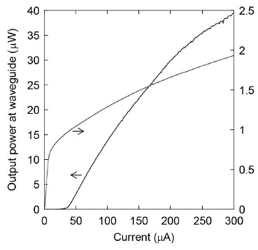
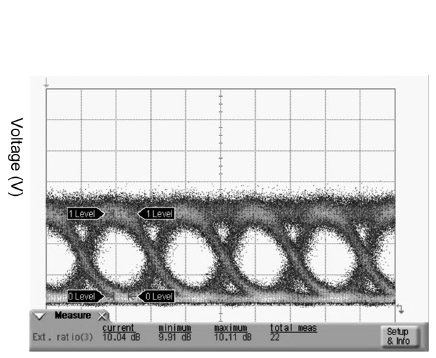
We measured a light output and an applied voltage versus an injected current, and the result is shown in Fig. 1. We obtained a threshold current of 32 µA, and the maximum output power was 39.3 µW at a current injection of 300 µA. There was an optical coupling loss of approximately 8 dB, and the plot shows calibrated output power at the waveguides. We then drove the LEAP lasers with a pseudo-random bit sequence of 231 – 1 at a bit rate of 10 Gb/s. Output light was monitored by a digital sampling oscilloscope via an optical amplifier that was used to compensate an optical coupling loss. Figure 2 shows the eye diagram of the LEAP lasers. We needed only 80-µA current injection to achieve a clear eye opening with an extinction ratio of 10 dB. We achieved the energy consumption of smaller than 10 fJ/bit under this operating condition.
Part of this work was supported by the New Energy and Industrial Technology Development Organization (NEDO).
- [1]
- D. A. B. Miller, proc. IEEE 97 (2009) 1166.
- [2]
- K. Takeda et al., Nature Photon. 7 (2013) 569.
- [3]
- S. Matsuo et al., JSTQE 19 (2013) 4900311.
 |
 |
- Fig. 1.
- L-I-V characteristic of the LEAP laser.
|
|
- Fig. 2.
- 10-Gb/s eye diagram.
|
|
<< Prev | Contents | Next >>