Bulk silicon has an indirect band gap and a multiple degenerate valley structure in the conduction band. Since photons do not carry significant momentum and a dipole transition requires momentum conservation, a direct optical transition is not allowed in bulk silicon. Here we demonstrate electric tuning of direct/indirect optical transitions with specially prepared Si/SiO2 interfaces [1], where the valley splitting is tuned by a gate electric field and its value is at least one order of the magnitude larger than that at an ordinary metal oxide semiconductor (MOS) interface [2]. For conventional Si MOS interfaces, the valley splitting is well explained by the extended zone effective mass theory [3], where real space confinement causes valley interaction. By extending this theory, it is expected that the valley splitting will lead to phononless direct optical transitions in Si. We therefore anticipate that the direct optical transition is significant and it can be controlled by the gate electric field in the interface with the large valley splitting.
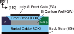
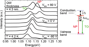
Devices are Si MOS field effect transistors with 4.3- or 6-nm-thick Si quantum well (QW) fabricated on SIMOX (separation by implantation of oxygen) (001) wafer annealed at 1350 °C for 40 hours. It is known that large valley splitting appears when electrons are squeezed to the buried oxide interface of SIMOX. Heavily doped p- and n-type contacts are formed in order to inject holes and electrons into a channel (Fig. 1). The front (FG) and back gate (BG) control the distribution of both carriers in the Si QW. Figure 2 shows typical electroluminescence (EL) spectra at various back-gate voltages (VBG). For VBG < 0, an indirect TO phonon mediated optical transition dominates the EL spectra, where the valley splitting (2Δ) is at most several mili-electron volts. In contrast, for VBG > 0, the EL intensities of phononless direct optical transition (NP) become dominant with increasing VBG. The intensity ratio of NP to bulk NP (the NP intensity at VBG = 0 V for the device with thicker QW) reached 800 at VBG = 80 V, where the valley splitting is estimated to be 30 meV. Thus we demonstrate electric tuning of direct/indirect optical transitions in Si just by changing gate voltage.
This work was partly supported by the Funding Program for Next Generation World-Leading Researchers of JSPS.