Integrated photonics technology has proven useful for the large-scale integration of quantum information systems on photonic chips thanks to its compactness and interferometric stability. Intense study is under way on the development of on-chip quantum components, such as quantum light sources [1], quantum circuits [2], and single photon detectors [3]. The next step is the integration and interconnection of these components on a single substrate. This time we have realized the monolithic integration of a Si waveguide photon pair source and a photon-pair demultiplexer employing a silica-based arrayed waveguide grating (AWG) [4], which can facilitate interconnecting the quantum light source and the circuit.
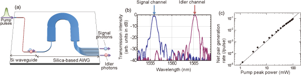
The circuit is schematically depicted in Fig. 1(a). In the silicon waveguide part, a correlated pair of signal and idler photons is created via spontaneous four-wave mixing process following the annihilation of two photons inside the pump pulse. Thanks to the high material nonlinearity of Si as well as the strong light confinement of the waveguide, non-degenerate photon pairs are efficiently created in the telecommunication wavelength. The photon pairs are subsequently spectrally separated [Fig. 1(b)] by AWG into different output channels. We employed silica-based material (SiOx), which is a low nonlinear material, as the core of the AWG in order to mitigate noise photon generation outside of the photon pair source. The integration of the two quantum photonic components has been realized with the monolithic photonic integration technology [5]. Using the device, we have successfully demonstrated the on-chip generation and demultiplexing of quantum correlated photons on a chip [Fig. 1(c)]. Furthermore, we have confirmed that the silica part of the device does not contribute to noise photon generation.
The device can be used as a compact correlated photon pair source, and will be useful for many quantum information applications including wavelength-division multiplexing quantum communication technologies and heralded single photon sources. Moreover, the silica-based AWG can provide an interface between a Si-based photon pair source and silica-based lightwave circuits, which are useful as linear-optics-based quantum circuits.