Semiconductor nanowires (NWs) have provided a new platform for fundamental physics research and have become next-generation building blocks in photonics, electronics, and energy conversion. One crucial challenge for NWs has been the development of a CMOS-compatible synthesis approach which produces semiconductor heterostructure NWs with excellent optical properties. This remains challenging because gold (Au), which is widely used as a catalyst particle when NWs are synthesized with the bottom-up vapor-liquid-solid (VLS) approach, is not permitted in the mainstream CMOS process.
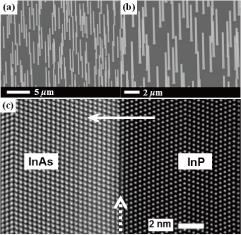
Here, we report gold-free multi-stacked InAs/InP heterostructure NWs with controlled luminescence wavelength in 1.1-1.6 µm. We realized the NW by using an indium-particle-assisted VLS synthesis approach [1-3]. The growth temperature as low as 320°C enables in the formation of an atomically abrupt InP/InAs interface by supressing the diffusion and weakening the reservoir effect in the indium droplet (Fig. 1). The low growth temperature also enables us to grown multi-stacked InAs/InP NWs in the axial direction without any growth on the NW side face in the vapor phase epitaxy mode.
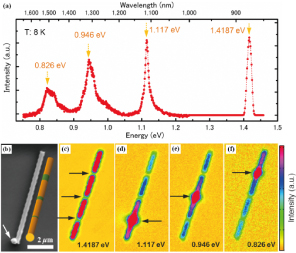
The high controllability of the growth technology ensures that the luminescence can be tailored by the thickness of InAs segment and cover the 1.3-1.5 μm telecommunication window range. By using the nanoscale-spatial-resolution technology combing CL with SEM, we directly correlated the site of different-thickness InAs segments with its luminescence property in a single NW and demonstrate the InAs-thickness controlled energy of optical emission in 1.1-1.6 μm (Fig. 2).
This work was supported by KAKENHI.