Observing Semiconducting Band-gap Alignment in MoS2 Layers Using a MoS2/SiO2/Si Heterojunction Tunnel Diode
The performance of Si transistors, the main fundamental devices in logic circuits, increases with miniaturization. When their size reaches from a few to ten nanometers, they gain new functionalities, such as single-electron manipulation [1], high-sensitivity charge detection [2], and photo emission [3]. However, even as miniaturization proceeds, it is essentially impossible to change the fundamental characteristics of Si material. On the other hand, graphene and other two-dimensional layered materials have been actively studied due to their remarkable characteristics, such as high carrier mobility and transparency. However, such materials still face technological difficulties for their applications. Therefore, we have been studying new devices that integrate Si and two-dimensional layered material in order to combine their remarkable characteristics. In this work, we demonstrate a tunnel diode composed of Si and MoS2 [4].
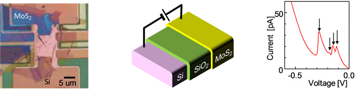
The tunnel diode is based on a Si transistor, except that its gate terminal is replaced with multiple-layer MoS2 film as shown in Fig. 1. This MoS2 film is formed on the Si channel by means of an exfoliation method using a bulk MoS2. The Si channel and MoS2 film have p-type and n-type transistor characteristics, respectively. Since there is a gate oxide SiO2 between the Si channel and MoS2 film, a p/insulator/n heterostructure is constructed (Fig. 2). Since the SiO2 is thin (6 nm), tunnel current flows between the Si and MoS2 when voltage is applied between them as shown in Figs. 2 and 3. Multiple current peaks indicating negative differential resistance (NDR) are clearly observed at room temperature. The mechanism of NDR is the same as that in a tunnel or Esaki diode composed of heavily doped p-n junctions, though current tunnels through the SiO2 layer in our device. The appearance of the four NDR peaks originates from the fact that the MoS2 film has four areas of different thickness and that the bandgap of layered MoS2 varies with its thickness. From voltages giving NDR peaks, we can evaluate the energy-band alignment of the heterostructure in our device. Using the heterostructure even for other two-dimensional layered materials, we can obtain information about their energy-band structure in a simple system under various conditions, e.g., low temperature and magnetic field. The heterostructure is also promising for new functional devices.
- [1] K. Nishiguchi et al., Appl. Phys. Lett. 88, 183101 (2006).
- [2] K. Nishiguchi et al., Jpn. J. Appl. Phys. 47, 8305 (2008).
- [3] J. Noborisaka, K. Nishiguchi, and A. Fujiwara, Sci. Rep. 4, 6940 (2014).
- [4] K. Nishiguchi et al., Appl. Phys. Lett. 107, 053101 (2015).
|
||
| Fig. 1. Photograph of the fabricated device. | Fig. 2. Schematic view of the device. | Fig. 3. Current characteristics. |