Gate-controlled Semimetal - Topological Insulator Transition in an InAs/GaSb Heterostructure
Topological insulators (TIs) are new states of matter that cannot be classified into any existing categories of materials. The insulating state in TIs cannot continue to the normal insulating state outside, and it is therefore necessary to break the insulating states. As a result, a conductive channel arises at the boundary of a TI. Electron scattering in this topologically protected conductive channel is restricted. Particularly, for two-dimensional (2D) TIs, dissipationless transport is expected. Therefore, TIs are promising for low power consumption electric devices.
Thus far we have succeeded in artificially realizing a 2D TI arising from the heterojunction between InAs and GaSb, which both are commonly used in III-V semiconductors [1]. Recently, we have further achieved in-situ semimetal-TI transition by applying a gate voltage between the gates on both the substrate and surface sides of an InAs/GaSb heterostructure [2]. This adds new functionality to TIs, which would enhance their device application.
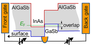
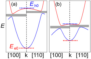
Figure 1 shows the energy band profile of the InAs/GaSb heterostructure with front (surface side) and back (substrate side) gates. Due to the hybridization between the conduction band of InAs and valence band of GaSb through the heterointerface, the topologically nontrivial different energy gap opens. The energy overlap between the conduction and valence bands can be controlled by applying a gate voltage on both sides. When the overlap is large enough the system becomes semimetallic as a result of the anisotropy of the GaSb valence band
[Fig. 2(a)]. By increasing the back gate voltage, the overlap becomes smaller and the band structure becomes that of a TI [Fig. 2(b)].
This work was supported by JSPS KAKENHI Grant No. 26287068.
- [1] K. Suzuki, Y. Harada, K. Onomitsu, and K. Muraki, Phys. Rev. B 87, 235311 (2013).
- [2] K. Suzuki, Y. Harada, K. Onomitsu, and K. Muraki, Phys. Rev. B 91, 245309 (2015).
|
|
| Fig. 1. Energy band profile of the InAs/GaSb heterostructure with front (surface side) and back (substrate side) gates. | Fig. 2. Schematic illustrations of dispersion relations for (a: semimetallic) large energy band overlap case and (b: TI) small overlap case . |