Atmospheric Pressure Chemical Vapor Deposition Growth of Millimeter-scale Single-crystalline Graphene on the Copper Surface with a Native Oxide Layer
Graphene fabricated by "bottom-up" methods always contains various kinds of structural defects, which are introduced during the fabrication process. For example, 1 mm2 chemical vapor deposition (CVD) grown graphene can be composed of over ten thousand single crystalline domains and centimeter-long domain boundaries [1]. These domain boundaries, as well as lattice defects, have been identified as main disorders to affect the electrical and mechanical performance of graphene. Thus, fabrication of large scale single crystalline graphene is important for its potential technological applications in nanoelectronics and related fields.
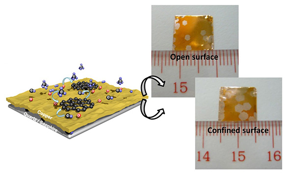
Here, we present an atmospheric pressure CVD approach to synthesize millimeter-scale graphene single crystals on commercial Cu foils [2]. A hydrogen-excluded annealing step is used to flatten the Cu surface and maintain the native oxide layer, which is catalytic inactive and is used to restrict the nucleation of graphene on Cu surface in the following growth process. A resulted density of ~12 nuclei cm–2 is obtained with an optimized annealing period. Combined with the annealing step, the growth of graphene is further modified by placing the catalyst foils on roughness-defined solid supports (quartz or sapphire), which generate two different types of reaction space: open and confined space on the double sides of the foils. Due to the variation in the kinetics role of oxide layer, reproducible results are observed that the domain size of as-grown graphene is larger on the confined surface, as shown in Fig. 1. With a polished quartz support, ~3 mm isolated graphene islands with an average growth rate of ~25 μm/min are achieved. The as-grown hexagonal domains are confirmed to be single-crystalline monolayer graphene with a field-effect mobility of ~4900 cm2/Vs at room temperature.
- [1] S. Wang et al., Nanoscale 6, 13838 (2014)
- [2] S. Wang et al., Chem. Mater. 28, 4893 (2016).
|
| Fig. 1. Schematic and optical images of single crystalline graphene domain grown on the Cu surface w/ and w/o support under same CVD procedure. |