A Planar Cold Cathode Based on Multilayer-graphene/SiO2/Si Heterostructure
Cathodes that emit electrons are used for various applications such as electron microscopy, electron beam lithography, material reformation, and vacuum gauges. The most commonly used cathode is a hot cathode that uses a filament heated up by current, and a Spindt-type cathode composed of a sharp cone [1] has been studied as a cold cathode with high functionality. While each cathode type has some advantages, there are also some problems: cathodes operate by using a high voltage supply in a high vacuum and electrons emitted spread widely; both of which lead to complicated systems. In this work, we demonstrated a planar cold cathode based on a multilayer-graphene/SiO2/Si heterostructure [2] to solve these problems.
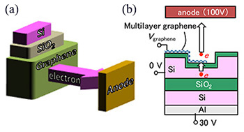
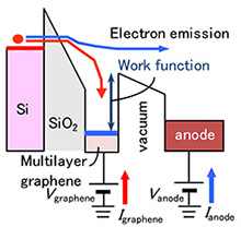
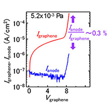
Figure 1 shows the schematic and cross-sectional views of the cold cathode based on a multilayer-graphene (~10 nm)/SiO2 (6 nm)/Si heterostructure. Figure 2 shows the mechanism of electron emission from the cathode. When voltage Vgraphene is applied to the multilayer graphene, electrons in the Si layer tunnel to the multilayer graphene through the SiO2. Electrons with energy larger than the work function (~5 eV) of the multilayer graphene are emitted from it to a vacuumed space and reach the anode, which leads to current Ianode. However, when the energy of electrons in the multilayer grapheme is smaller than its work function, the electrons (current Igraphene) flow into the multilayer graphene without electron emission. Figure 3 shows the electron-emission characteristics. The increase in Vgraphene increases the tunneling current Igraphene. At Vgraphene larger than the work function of the multilayer-graphene, Ianode flows because the electrons are emitted from the cathode and reach the anode. The electron-emission efficiency is defined as 0.3%, which is four orders of magnitudes larger than in our previous results using polycrystalline Si instead of multilayer graphene [3]. This improvement originates from a small scattering of electrons in the multilayer graphene due to its thinness, which means that single-layer graphene is promising for further improvement of the efficiency. On the other hand, since multilayer-graphene’s conductivity is not sensitive to electron-emission characteristics, wide graphene grown by chemical vapor deposition can be used to make a wide-area cathode. Additionally, since electrons are emitted perpendicular to the multilayer graphene with a small voltage in low vacuum, a simple system for electron emission targeting various applications can be achieved.
- [1] C. A. Spindt, J. Appl. Phys. 39, 3504 (1968).
- [2] K. Nishiguchi et al., Appl. Phys. Express 9, 105101 (2016).
- [3] K. Nishiguchi et al., Jpn. J. Appl. Phys. 47, 5106 (2008).
|
|
|
| Fig. 1. (a) Schematic and (b) cross-sectional view of the cathode. | Fig. 2. A mechanism of electron emission. | Fig. 3. Electron-emission characteristics. |