Engineering Quantum Spin Hall Insulators by Strained-layer Heterostructures
Quantum spin Hall insulators (QSHIs) have insulating bulk and conductive edges originating from nontrivial inverted band structures. Owing to these unique properties of the spin-helical edge modes, QSHIs have been proposed as a platform for exploring spintronics applications and exotic quasiparticles useful for topological quantum computation. InAs/GaSb quantum wells (QWs) have been predicted to offer a QSHI and have a key advantage of being in situ tunable between trivial and topological insulating phases. However, the residual bulk conductivity associated with the small energy gap in the QSHI phase has been an obstacle to the unambiguous identification of edge properties. In this study, we propose a strained InAs/InGaSb heterostructure as a QSHI candidate and demonstrate that the strain enhances the energy gap and leads to superior bulk insulation properties [1].
The QWs were grown by MBE and comprise InAs with the thickness of t (8.5~10.9 nm) and 5.9-nm-thick In0.25Ga0.75Sb layers, sandwiched between AlSb barrier layers. Compressive strain induced in the InGaSb layer enhances heavy-hole light-hole splitting and impacts the energy dispersion in the QSHI phase.
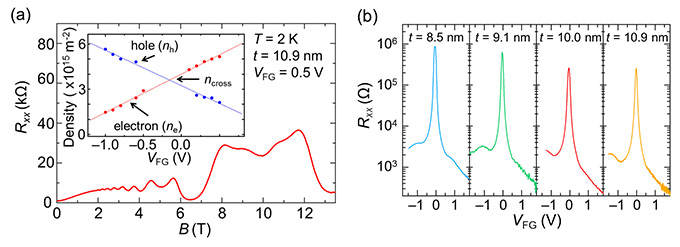
We determined the density of electrons (ne) and holes (nh) separately through the fast Fourier transform (FFT) analysis of the longitudinal resistance (Rxx) vs. magnetic field (B) trace [Fig. 1(a)]. We confimed the coexsitence of electrons and holes at high densities, which indicates that the QW is deep in the band-invered regime. From the linear fit of gate voltage (VFG) dependence of ne and nh (inset), we obtained the density ncross at the charge neutrality point (where ne = nh) to be 3.6 × 10¹⁵ m–2, which gives a quantitative measure of the band overlap. We emphasize that the linear fit in the two-carrier regime gives an accurate evaluation of the band overlap.
The Rxx peak height at the the charge neutrality point, which mainly reflects in-gap states in the bulk, increased with decreasing InAs thickness and reached 889 kΩ (corresponding resistivity of ~10h/e2) [Fig. 1(b)]. All samples have bulk resistivity two orders of magnitude higher than those of the InAs/GaSb system. These results demonstrate that InAs/InGaSb strained QWs are promising for investigating edge transport properties.
This work was supported by JSPS KAKENHI JP15H05854 and JP26287068.
- [1] T. Akiho et al., Appl. Phys. Lett. 109, 192105 (2016).
|
| Fig. 1. (a) Rxx vs. B trace. (Inset) VFG dependence of ne and nh. (b) Rxx peaks with different InAs thickness. |