All-optical switch using photonic crystal nanocavity
Background
 Since photons interact each other through the dipole moment,
to obtain an efficient photon-photon interaction it is important to
achieve large coefficient between the material and photons. However, the
optical devices are usually made with optically transparent materials,
which have only small light-matter interaction
coefficient. Recently it is known that by designing the structure of
the optical device, it is possible to overcome this fundamental
problem. By introducing a new structure that can maximize the photon density,
we can effectively enhance the light-matter interaction.
Since photons interact each other through the dipole moment,
to obtain an efficient photon-photon interaction it is important to
achieve large coefficient between the material and photons. However, the
optical devices are usually made with optically transparent materials,
which have only small light-matter interaction
coefficient. Recently it is known that by designing the structure of
the optical device, it is possible to overcome this fundamental
problem. By introducing a new structure that can maximize the photon density,
we can effectively enhance the light-matter interaction.
An optical cavity is a good candidate to yield a high
photon density, because it can confine the light through a long period
of time in one place. The quality factor (Q-factor) gives the extent
of the light confinement. To obtain a higher density of photons, one
can reduce the size of the cavity. However, it has been regarded as a
difficult task to keep the Q while reducing the mode volume V by using
conventional light confinement method. Yet it is now possible to
obtain large Q/V value by employing light confinement yielding
photonic bandgap (PBG).
Originality
We fabricated high-Q photonic crystal nanocavity using silicon
photonic crystal slabs. We showed that <100 ps switching is
possible using this device. Moreover, the operating energy is
about 100 fJ. (1 pico = 1 x 10-12, 1 femto =1 x
10-15).
This energy value is the smallest yet reported for an all-optical switching device using silicon.
Impact
Silicon is one of the most promising material owing to the high fusion
with conventional planer semi-conductor processing. This work is
significant because the ultra-low energy optical switching is
demonstrated using silicon. In addition, since all the light propagate
in-the-plane of the chip this study paves the way to the development
of the nano-scale all-optical signal processing.
Operation principle
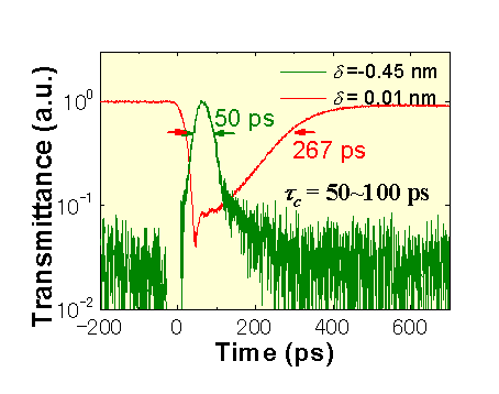 At the moment a control pulse injects the cavity, the refractive
index of the silicon changes due to the carriers generated by
two-photon absorption. When the signal light is initially at the
resonance of the nanocavity, the cavity transmittance of the signal light exhibit ON state.
When carriers are generated, the signal transmittance exhibit OFF state because the wavelength of the signal light
and the resonance of the nanocavity becomes different. By
detuning of the signal light to a shorter wavelength, we can also
perform OFF to ON modulation.
At the moment a control pulse injects the cavity, the refractive
index of the silicon changes due to the carriers generated by
two-photon absorption. When the signal light is initially at the
resonance of the nanocavity, the cavity transmittance of the signal light exhibit ON state.
When carriers are generated, the signal transmittance exhibit OFF state because the wavelength of the signal light
and the resonance of the nanocavity becomes different. By
detuning of the signal light to a shorter wavelength, we can also
perform OFF to ON modulation.
References
- T. Tanabe, M. Notomi, A. Shinya, S. Mitsugi, and E. Kuramochi,
"All-optical switches on silicon chip realized using photonic
crystal nanocavitites," Appl. Phys. Lett. 87, 151112 (2005).
- T. Tanabe, M. Notomi, A. Shinya, S. Mitsugi, and E. Kuramochi,
"Fast on-chip all-optical switches and memories using silicon photonic
crystal with extremely low operating energy," Quantum Electronics and
Laser Science Conference (QELS'05), QPDA5, Baltimore, May 22-27,
(2005).
 | ©2005
NTT Basic Research Laboratories
| ©2005
NTT Basic Research Laboratories