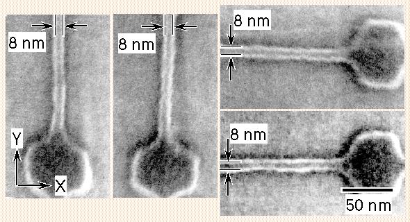
Sub-10-nm Patterning using Alumina-Gel Resists

- To achieve a high resolution and high overlay
accuracy, we are developing new electron beam lithography systems. By using the system and an alumina-gel
resist, we have already realized 8-nm-wide
lines.
References
- K. Yamazaki, M. S. M. Saifullah, H. Namatsu,
and K. Kurihara, ''Sub-10-nm
Lithography with Sub-10-nm Overlay Accuracy,
'' Proc. SPIE. 3997, (2000)
in printing.
- M. S. M. Saifullah, H. Namatsu, T. Yamaguchi,
K. Yamazaki, and K. Kurihara,
''Spin-coatable Al2O3 resists in electron
beam nanolithography,''
Proc. SPIE. 3678, pp. 633--642, 1999.
- M. S. M. Saifullah, H. Namatsu, T. Yamaguchi,
K. Yamazaki, and K. Kurihara,
''Effect of chelating agents on high resolution
electron beam nanolithography
of spin-coatable Al2O3 gel films,'' Jpn.
J. Appl. Phys. 38,
pp. 7052--7058, 1999.
- K. Yamazaki, A. Fujiwara, Y. Takahashi, H.
Namatsu, and K. Kurihara,
''Sub-10-nm overlay accuracy in electron
beam lithoraphy for nanometer-scale
device fabraication,'' Jpn. J. Appl. Phys.
37, pp. 6778--6791,
1998.
Back
Nanostructure Technology Research Group Home
Page