|
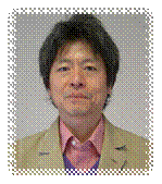
Dr. Kouta Tateno |
|||||||||||
|
|
|||||||||||
|
Thin-Film
Materials Research Group Materials
Science Laboratory NTT
Basic Research Laboratories / NTT Nanophotonics Center |
|||||||||||
|
Biography |
|||||||||||
|
Kouta Tateno was
born in He
is a member of the Japan Society of Applied Physics and the Electrochemical
Society of Japan. |
|||||||||||
|
Research Interest |
|||||||||||
Artificial photosynthesis is also my interest.
Nanowires should play an important role in photoelectric CO2 reduction. |
|||||||||||
|
|
|||||||||||
|
|
|||||||||||
|
|
|||||||||||
