 Welcome to Yoshitaka Taniyasu's Homepage

Biography
1996 Bachelor degree from the division of Electrical and Electronic
Engineering, Chiba University, Japan
1998 Master degree from the division of Electronic and Mechanical
Engineering, Chiba University, Japan
2001 Ph.D in Engineering from Chiba University
(Doctor thesis: In-situ monitoring of MOVPE growth of III-nitride
semiconductors by spectroscopic ellipsometry)
2001-2003 Research associate, NTT Basic research laboratories, Japan
2003- NTT Basic research laboratories
2010-
Distinguished Technical Member of NTT Basic Research Laboratories
2011-2012 Visiting
Researcher at Ecole polytechnique
fédérale de Lausanne (EPFL), Switzerland
News
Ø
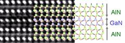
“Polarization property of deep-ultraviolet light emission
from C-plane AlN/GaN short-period superlattices”
published in Appl. Phys. Lett.
99, 251112 (2011).
Ø
Young
Scientist Award, The International Symposium on Compound Semiconductors 2011
Ø
Young
Scientists’ Prize, The Minister of Education, Culture, Sports, Science and Technology
(MEXT),
 Research
Interests
Research
Interests
III-V Nitride Semiconductors and
Devices
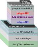
1. AlN-based ultra-violet light-emitting devices
2. MOVPE growth technologies
3. Physical properties of AlN-based
materials
Selected Publications
AlN-based ultra-violet light-emitting diodes (UV-LEDs)
·
Y. Taniyasu and M. Kasu, “Polarization
property of deep-ultraviolet light emission from C-plane AlN/GaN
short-period superlattices”, Appl.
Phys. Lett. 99, 251112 (2011).
·
Y. Taniyasu and M. Kasu, “Origin
of exciton emissions from an AlN
p-n junction light-emitting diode”, Appl. Phys. Lett. 98, 131910 (2011).
·
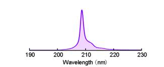
Y. Taniyasu and M. Kasu, “Surface
210 nm light emission from an AlN p–n junction
light-emitting diode enhanced by A-plane growth orientation”, Appl. Phys. Lett. 96, 221110
(2010).
·
Y. Taniyasu, M. Kasu, and T. Makimoto, “An aluminium nitride
light-emitting diode with a wavelength of 210 nanometres”,
Nature 441, 325-328 (2006).
Emission properties
·
R. A. R. Leute, M. Feneberg, R. Sauer, K. Thonke, S.
B. Thapa, F. Scholz, Y.
Taniyasu and M. Kasu, “Photoluminescence of highly
excited AlN: Biexcitons and
exciton-exciton scattering”, Appl.
Phys. Lett.
95, 031903 (2009).
·
Y. Taniyasu, M. Kasu, and T. Makimoto, "Radiation and polarization properties of
free-exciton emission from AlN
(0001) surface”, Appl. Phys. Lett.
90, 261911 (2007).
·
G. M. Prinz, A. Ladenburger, M. Schirra, M. Feneberg, K. Thonke, R. Sauer, Y.
Taniyasu, M. Kasu, and T. Makimoto,
“Cathodoluminescence, photoluminescence, and
reflectance of an aluminum nitride layer grown on silicon carbide substrate”, J.
Appl. Phys. 101, 023511 (2007).
Doping mechanisms and carrier transport
properties
·
Y. Taniyasu, M. Kasu, and T. Makimoto, “Increased electron mobility in n-type Si-doped AlN by reducing dislocation density”, Appl.
Phys. Lett. 89, 182112 (2006).
·
Y. Taniyasu, M. Kasu, and T. Makimoto, “Electrical conduction properties of n-type
Si-doped AlN with high electron mobility (> 100cm2V-1S-1)”,
Appl. Phys. Lett. 85, 4672
(2004).
·
Y. Taniyasu, M. Kasu, K. Kumakura, T. Makimoto, and N.
Kobayashi, “High electron concentrations in Si-doped AlN/AlGaN
superlattices with high average Al content of 80%”, phys. stat. sol. (a) 200, 40 (2003).
·
Y. Taniyasu, M. Kasu, and N.
Kobayashi, “Intentional control of n-type conduction for Si-doped AlN and AlXGa1-XN (0.42 < x
< 1)”, Appl. Phys. Lett.
81, 1255 (2002).
AlN-based cold cathode materials and it applications
·
Y. Taniyasu, M.Kasu, and T. Makimoto, “Field emission properties of heavily Si-doped AlN in triode-type display structure”, Appl.
Phys. Lett. 84, 2115 (2004).
·
Y. Taniyasu, M. Kasu, and N. Kobayashi, “Lattice parameters
of wurtzite Al1-XSiXN ternary
alloys”, Appl. Phys. Lett.
79, 4351 (2001).
MOVPE growth mechanisms
·
Y. Taniyasu, M. Kasu, and T. Makimoto, "Threading dislocations in heteroepitaxial AlN layer grown
by MOVPE on SiC (0001) substrate", Journal of
Crystal Growth 298, 315 (2007).
·
Y. Taniyasu and A. Yoshikawa,
“In-situ Monitoring of Surface Stoichiometry and
Growth Kinetics Study of GaN (0001) in MOVPE by Spectroscopic Ellipsometry”, J. Elect. Mater.
30, 1402 (2001).
Nitride / Diamond heterostructure
·
K. Hirama, M. Kasu,
and Y. Taniyasu, "RF High-Power Operation of AlGaN/GaN
HEMTs Epitaxially Grown on
Diamond ", IEEE Electron Device Letters 33,513 (2012).
·
K. Hirama, Y. Taniyasu, and M. Kasu, “AlGaN/GaN high-electron
mobility transistors with low thermal resistance grown on single-crystal
diamond (111) substrates by metalorganic vapor-phase epitaxys”, Appl. Phys. Lett. 98, 162112 (2011).
·
K. Hirama, Y. Taniyasu, and M. Kasu, “Electroluminescence and capacitance-voltage
characteristics of single crystal n-type AlN
(0001)/p-type diamond (111) heterojunction diodes”, Appl. Phys. Lett. 98, 011908
(2011).
·
K. Hirama, Y. Taniyasu, and M. Kasu, “Heterostructure growth of
a single-crystal hexagonal AlN (0001) layer on cubic
diamond (111) surface”, J. Appl. Phys. 108, 013528
(2010).
·
Y. Taniyasu and M. Kasu,
"MOVPE growth of single-crystal hexagonal AlN on
cubic diamond", Journal of Crystal Growth 311, 2825-2830 (2009).
Polytype control: Cubic InGaN LED
·
Y. Taniyasu, K. Suzuki, D. H.
Lim, A. W. Jia, M. Shimotomai,
Y. Kato, M. Kobayashi, A. Yoshikawa, and K. Takahashi, “Cubic InGaN/GaN Double-Heterostructure
Light Emitting Diodes Grown on GaAs (001) Substrates
by MOVPE”, phys. stat. sol. (a) 180,
241 (2000)
Awards
u
Young
Scientist Award
“Seminal Contributions to the Growth of AlN and its Application to the Shortest Wavelength Light
Emitting Diodes”
The International
Symposium on Compound Semiconductors 2011
The Minister of
Education, Culture, Sports, Science and Technology (MEXT),
u
Young
Scientist Award
“For outstanding contributions in
developing and implementing Aluminum Nitride deep-ultraviolet light-emitting
diodes”
14th Semiconducting and Insulating Materials Conferences (SIMC
XIV)
u
Young
Scientist Award for the Presentation of an Excellent Paper at Japan Society of
Applied Physics (JSAP) meeting
Research Funding
Grant-in-Aid for
Young Scientists (A) from MEXT (The Ministry of Education, Culture, Sports,
Science and Technology),
Period: Apr. 2007
- Mar. 2010 (3 years)
Conference committee
Ø
International
Workshop on Nitride Semiconductors (IWN2006, 2012) Program committee member
Ø
Second
International Symposium on Growth of III-Nitrides (ISGN-2) Program committee
member
Ø
Conference
on Lasers and Electro-Optics (CLEO 2009, 2010, 2011, 2012, 2013) Program committee
member
Ø
The
Pacific Rim Conference on Laser and Electro-Optics 2013 (CLEO-PR) Program committee
member
3-1 Morinosato Wakamiya, Atsugi-shi,
Kanagawa, 243-0198