Satoru Suzuki, and Yoshihiro Kobayashi
Materials Science Laboratory
Å@Carbon nanotubes are one of the most promising materials
for future nanoelectronics, because of the nanometer-scale structure and the
unique electronic properties. Actually, a nanotube-based field effect transistor
and single electron transistor have been demonstrated to overcome a Si device.
For fabricating a nanotube-based integrated circuit, it is necessary to place
nanotubes only at specified positions. However, high-density nanotube growth
almost always results in the growth of unnecessary nanotubes at unspecified
positions, which would cause short circuits, because controlling the growth
direction of individual nanotubes is still impossible. Thus, selective removal
of carbon nanotubes from a nanotube network is a crucial issue for fabricating
an integrated circuit.
Å@Recently, we found that low-acceleration-voltage electron irradiation induces
significant damage in single-walled carbon nanotubes (SWNTs). Moreover, we
developed a simple method for removing unnecessary nantoubes selectively utilizing
the low-acceleration-voltage electron irradiation damage.
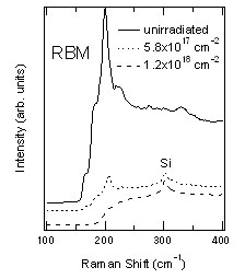
Å@Raman spectra of SWNTs before and after electron beam irradiation is shown
in Fig. 1. The acceleration voltage was 1 kV. The electron irradiation drastically
decreased the radial breathing modes (RBM) intensity, which is characteristic
in the quasi-one-dimensional structure of SWNTs, indicating that the irradiation
caused structural damage in the SWNTs [1]. This damage was found to be extensively
caused at around 1 kV. Although SWNTs are chemically highly stable, the electron
irradiation significantly reduces the chemical stability. This enables us
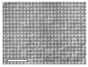
to simply remove the damaged SWNTs selectively. A typical example of suspended
SWNTs after the selective removal procedure is shown in Fig. 2. The SWNTs
were grown on Si pillars having diameters of 200 nm. The electron beam was
scanned along the dashed line, and then, the sample was annealed in air. In
spite of the very simple procedure, the SWNTs initially crossing the line
were successfully removed. This technique would make it possible to fabricate
various kinds of nanotube circuits.
[1] S. Suzuki et al., Jpn. J. Appl. Phys. 43 (2004) L1118.
[2] S. Suzuki et al., Jpn. J. Appl. Phys. 44 (2005) L133.
 |
 |
|
| Fig. 1. Raman spectra of SWNTs before and after electron irradiation. | Fig. 2. SEM image of the suspended SWNT network after the selective removal procedure. The electron beam was scanned along the dashed line. Scale bar: 2.5 μm. |