Hiroki Hibino and Yoshio Watanabe*
Materials Science Laboratory
Approaches to fabricating semiconductor nanostructures
can be roughly classified into “top-down” lithography and “bottom-up” self-assembly.
Self-assembly has potential advantages of low cost, large scale, high quality,
and so on, but there still remain lots of problems to be solved, especially
in the controllability of the size and position of nanostructures. Our group
has developed novel self-organized nanostructure fabrication methods through
atomic scale control of semiconductor surface structures. Here, we demonstrate
that Au-Si alloy islands are self-assembled in a controlled manner using an
atomic step array on Si(111) as templates.
We formed three-dimensional (3D) islands on Si(111) by Au deposition at high
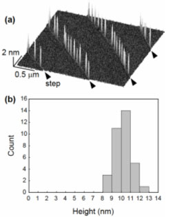
(~700℃) and then at low (~400℃) temperatures. Figure 1 shows an atomic force
microscopy (AFM) image of the islands and their height distribution. 3D islands
with a relative deviation of 10% are arranged at atomic steps. Real-time observations
of the island formation using low-energy electron microscopy (LEEM) revealed
that the islands formed within a narrow Au coverage window, resulting in the
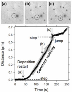
narrow size distribution. The islands were allowed to coarsen by interrupting
the Au deposition. When the Au deposition was resumed, the islands moved into
upper terraces leaving trenches behind. This indicates that the islands are
Au-Si alloy droplets. Additionally, the islands moved on the terraces almost
at constant velocities, but when they approached the upper-side steps, they
jumped to the steps (Fig. 2). The atomic steps provide stable positions for
Au-Si alloy islands, which helps them to arrange at the steps.
We showed that the position and size of Au-Si alloy islands can be controlled
by using atomic steps as templates for island formation. Our method is very
simple because it does not include any lithographic techniques, and it is
useful for preparing substrates for semiconductor nanowire growth and attaching
functional molecules.
*Present address: NTT advanced technology Corporation
 |
 |
|
Fig. 1.
AFM image of 3D islands and their height distribution. |
Fig. 2. The moving distance
of the island indicated by the dotted circle in LEEM images (a)-(c)
as a function of time. |