Optical Science Laboratory
@Recently, the two-dimensional photonic crystal slab (PCS)
has attracted great interest because it has led to the development of high
quality-factor photonic nanocavities and low-loss waveguides [1]. It has been
revealed that a guided mode induced by a line defect in ideal PCS is theoretically
lossless when it is designed to be inside the photonic band gap and under
the light line. However, current nanolithography technology allows nanometer-order
disorder and it is believed that such disorder causes a considerable loss
increase due to out-of-plane scattering.
@One aim of our research is to demonstrate that waveguide loss can be reduced
by reducing fabrication disorder. We patterned PCSs by using a precise electron
beam lithography system with 1-nm position accuracy and 100-kV acceleration,
where we paid great effort to minimizing the proximity effect. We observed
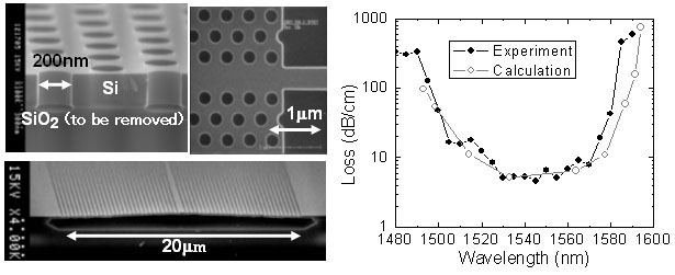
the fabricated Si PCS with scanning electron microscopes and found that disorder
(Ð, RMS) was about 3 nm (Fig. 1). We measured the propagation loss of PCS
waveguides by the cut-back method. The minimum loss measured was 5dB/cm (Fig.
2), which is record loss for photonic crystal waveguides [2].
@Another aim of our research is to reveal the physics of PCS waveguide loss.
We applied the photon Green function tensor (GFT) formalism [3] to disorder-related
scattering in the guided mode. We derived the loss formula as a simple product
of the disorder and local density of states of light between the initial state
and final state. We calculated the loss assuming Ð of 3nm, and the result
showed surprisingly good agreement with the experimental data (Fig. 2). This
loss calculation by our GFT method is the most detailed ever achieved. We
investigated the scattering-loss mechanism in detail by theory and experiment.
We revealed for the first time that the loss characteristics of PCS waveguides
are unique and complex because the loss mechanisms (out-of-plane scattering,
intermode scattering, and backward scattering) are tightly bound with photonic
band structure.
@In conclusion, by experiment and theory, we successfully revealed the detailed
physics of scattering loss in PCS waveguides caused by fabrication disorder.
[1] M. Notomi et al., Optics Express 12, 1551 (2004).
[2] E. Kuramochi et al., LEOS2004, WF6 (2004).
[3] S. Hughes et al., Phys. Rev. Lett. 94, 033903 (2005).
 |
||
| Fig. 1. SEM images of Si
PCSs fabricated in this study. |
Fig. 2. Measured and calculated loss
spectra of PCS waveguides. |
|