Optical Science Laboratory
Å@Small cavities with strong light confinement (high-Q) can
be fabricated by employing photonic crystals (PhCs) [1], whose dielectric
is periodically modulated. In such small high-Q optical cavities, efficient
all-optical modulation based on the light-matter interaction is expected because
the photon density inside the cavity becomes extremely high. Silicon-based
integrated optical circuits are regarded to have very high potential, due
to the possibility of fusion with existing electrical devices. However, there
has been some doubt as to whether active all-optical devices can satisfy certain
requirements, such as low operation energy, high-speed operation, high switching
contrast, and small device size. We will also have to be able to cascade them
on-chip. No device meeting these requirements has been fabricated on silicon
yet. Here, we demonstrated low operation energy and high-speed all-optical
switching on silicon-chip based on a PhC high-Q nanocavity [Fig. 1 (top)].
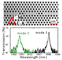
Å@The resonant transmission spectrum of a fabricated device under the linear
operation condition is shown in Fig. 1 (bottom). When the optical energy of
the near-infrared light is converted to thermal energy through the two-photon
absorption process, the center of the transmission spectrum of the nanocavity
shifts because the refractive index is modulated. By utilizing this phenomena,
ultra-low-energy switching operation of a few pJ (pico=10-12) is performed
[2]. By utilizing refractive index modulation due to the carrier-plasma effect,
further operation energy reduction and switching speed enhancement are expected.
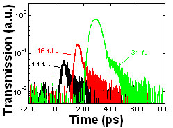
As shown on Fig. 2, the all-optical switching operation based on the carrier-plasma
effect is demonstrated at few ten fJ (femto=10-15) effective energy with a
speed higher than 100 ps [3]. In the case shown in the graph, continues-wave
signal light whose wavelength is slightly detuned to shorter wavelength from
Mode-S resonance is modulated with pulsed control light, which is Mode-C resonant.
This energy value and the device size are the smallest yet reported for fast
silicon all-optical active devices, and these are achieved owing to the high-Q
and efficient coupling with waveguides that are simultaneously attained in
our PhC nanocavities [2].
Å@The present result opens the way to silicon photonics; namely, the possibility
of practical high-speed, low-power, and high-density all-optical logic gate
on-chip applications on a silicon PhC platform.
[1] M. Notomi et al., Opt. Express 12 (2004) 1551.
[2] M. Notomi et al., Opt. Express 13 (2005) 2678.
[3] T. Tanabe et al., CLEO/QELS2005,QDPA5, Baltimore (2005) .
 |
 |
|
| Fig. 1. Electron microscope
image of the silicon PhC nanocavity (top). Linear transmission spectrum
(bottom). |
Fig. 2. Recorded switching operation
of the signal waveform as a function of the control pulse energy.
|