Optical Science Laboratory
Å@Recently, nanoprint-nanoimprint technologies or scanning
probe microscope (SPM) lithography is attracting attentions for the fabrication
of nanostructures used in electronic or optical devices. Compared to conventional
"projection-type" lithography, these "contact-type" lithographies
have advantages in size and ease of operation. However, because the basic
concept involves transferring the surface shape of a mold, the pattern cannot
be modified in nanoprint-nanoimprint technologies. SPM lithography, in which
an electrochemical reaction is induced by a conductive probe tip, can provide
pattern flexibility. However, the throughput is still low. We are trying to
develop a lithography technique that can provide good throughput and flexibility
simultaneously.
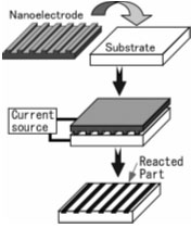
Å@Figure 1 shows the principle of nanoelectrode lithography. A nanoelectrode
surface consists of a conductive area and an insulating area. The nanoelectrode
makes contact with the surface of a target. When a voltage is applied, current
flows between the nanoelectrode and the target material. Then, an electrochemical
reaction occurs on the target surface. For example, anodic oxidation of the
semiconductor, Si or GaAs, transfers the pattern to the target [1, 2]. Figure
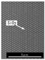
2 shows an example of Si substrate patterning by nanoelectrode lithography.
In Fig. 2, a nanoelectrode with a 300-nm-pitch dot pattern was used. The fabricated
oxide pattern worked well as a mask for wet and dry etching, which means that
resist-less patterning is possible. In addition, nanoelectrode lithography
does not deform the surface of the target during the patterning process. Therefore,
it will enable us to overwrite a pattern to fabricate a more complex pattern.
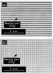
Figure 3 shows checked pattern fabricated by repeating the process with a
line-and-space (L/S) pattern [3].
Å@As shown here, nanoelectrode lithography has some advantages, such as direct
fabrication of the etching mask and modification of fabricated patterns by
combining this approach with another lithographic technique. In addition,
the lithography process can directly fabricate patterns defined by chemical
characteristics such as hydrophilic or hydrophobic properties. These pattern
may be used as templates for selective growth of semiconductors. We will apply
nanoelectrode lithography for patterning of metal layers or resist layers
on a substrate to prove the generality of the technique.
[1] A. Yokoo, Jpn., J. Appl., Phys., 42, L92 (2003)
[2] A. Yokoo, S. Sasaki, Jpn., J. Appl., Phys., 44, 1119 (2005)
[3] A. Yokoo, J. Vac. Sci. Technol. B, 21, 2966 (2003)
 |
 |
 |
|
Fig. 1 Nanoelectrode lithography |
Fig. 2 Fabricated pattern on Si |
Fig. 3 Multiple patterning (a) after 1st procedure (b) after 2nd procedure |