Å@
Kazuhide Kumakura and Toshiki Makimoto
Materials Science Laboratory
Å@Nitride-based semiconductors are promising materials for high-temperature or high-voltage operation devices because of their wide band gap. Heterojunction bipolar transistors (HBTs) are normally-off devices and can be operated with large current densities. Therefore, nitride-based HBTs are expected to operate at high temperature and with high power. However, dislocations or process-induced damage in nitride-based HBTs results in large leakage current and low breakdown voltage.
Å@We have developed a buffer layer for the growth of high-quality nitride-based
semiconductors on sapphire substrates [1]. Using the buffer layer and a
low-damage etching process, we have succeeded in the first operation of
Pnp AlGaN/GaN HBTs with a common-emitter configuration. In order to clarify
the transport mechanism at high-temperature, we investigated the current-voltage
(I-V) characteristics of the Pnp HBTs at temperatures ranging from room temperature (RT) to 590 Åé.
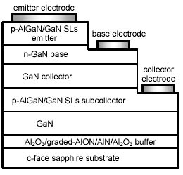
Å@We deposited Al2O3/graded-AlON/AlN/Al2O3 as a buffer layer on sapphire substrates by electron cyclotron resonance
(ECR) plasma sputtering at RT. The total layer thickness was 20 nm. Figure
1 shows the layer structure of the Pnp AlGaN/GaN HBTs grown on the substrate by metalorganic vapor phase epitaxy.
Emitter and base mesas were defined by lithography and ECR plasma etching.
Pd/Au and Al/Au were used as the ohmic contact metals for the p-type and n-type layers, respectively.
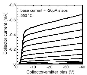
Å@Figure 2 shows the common-emitter I-V characteristics of the Pnp AlGaN/GaN HBT at 550 Åé [2]. Good saturation properties were observed
at this high-temperature and the leakage current was less than 1 µA
without the base current. The operation temperature is the highest among
semiconductor devices. The reason for this high-temperature operation is
ascribed to our techniques for high-quality growth of nitride-based semiconductors
and the low-damage process. These results indicate that nitride-based HBTs
are promising for high-power electronics.
[1]K. Kumakura, M. Hiroki, and T. Makimoto, Int. Workshop on Nitride Semiconductors
2004, P5.1, Pittsburgh, USA, 2004; J. Crystal Growth 292 (2006) 155-158.
[2]K. Kumakura and T. Makimoto, 2005 Int. Conference on Solid State Devices
and Materials, Kobe, Japan, I-6-2, 2005.
 |
 |
||||
|
|