Å@
Satoru Suzuki, Kenichi Kanzaki and Yoshihiro Kobayashi
Materials Science Laboratory
Å@A carbon nanotube can be metallic or semiconducting depending on its chirality. The band gap of semiconducting nanotubes strongly depends on their diameter. No technique has yet been established for controlling the chirality and diameter. This is a big problem in terms of nanotube applications for nanoelectronics. For example, a metallic nanotube does not work as a field effect transistor (FET).
Å@Recently, we have developed a simple technique for converting the electric
properties of a metallic nanotube to semiconducting [1]. The gate characteristics
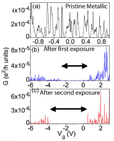
of a single-walled carbon nanotube (SWNT) FET at 28 K are shown in Fig.
1. The SWNT was originally metallic, so that there was no off-region in
the gate characteristics [panel (a)]. The oscillation of the conductivity
is caused by a Coulomb blockade specific to such a low temperature measurement.
When the device was irradiated by electrons of 1 keV up to a dose of Å`10-4 C/cm2, an off-region appeared [panel (b)]. Such gate characteristics are specific
to semiconducting SWNTs. Further irradiation widened the off-region [panel
(c)]. The irradiation-induced change of the gate characteristic is, in
appearance, similar to the change that would be caused by changing the
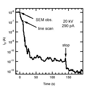
chirality and diameter. Moreover, as shown in Fig. 2, intensive irradiation
finally makes a SWNT almost completely insulating [2]. These results show
that the electric properties of SWNTs can be widely changed from metallic
to insulating by controlling the irradiation dose. Defects created in the
SWNTs by the irradiation play an essential role in the irradiation-induced
electric property change [3,4].
[1] A. Vijayaraghavan et al., Nano Lett. 5 (2005) 1575.
[2] S. Suzuki et al., Jpn. J. Appl. Phys. 44 (2005) L1498.
[3] S. Suzuki et al., Jpn. J. Appl. Phys. 43 (2004) L1118.
[4] S. Suzuki et al., Jpn. J. Appl. Phys. 44 (2005) L133.
 |
 |
|||||
|
Å@ |
|