Å@
Hiroo Omi and Tomoaki Kawamura
Materials Science Laboratory
Å@Nanoscale ultra-thin Si films exhibit quantum size effects when their
thickness becomes smaller than several nanometers. In order to control
nanoscale silicon devices based on the quantum size effect, it is essential
to achieve high-quality silicon nanolayers without strain distribution.
Ultrathin silicon nanolayers are usually fabricated by thermal oxidation
and HF etchback processes on silicon-on-insulator wafers. In this method,
the silicon layers are subjected to strain due to the difference in the
thermal expansion coefficients between Si and SiO2 during the thermal silicon oxidation. As a result, the strain significantly
increases as the silicon nanolayers become thinner, as has been observed
by X-ray diffraction and Raman spectroscopy. However, with these conventional
apparatuses, we can only detect information about the average lattice strain
in the silicon nanolayers; it is difficult to detect information about
the localized strains existing on the surface of the thin silicon nanolayers
or at the Si/SiO2 interfaces.
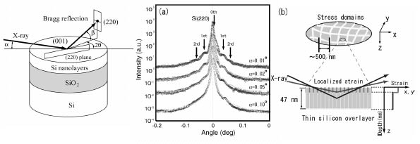
Å@We developed a new apparatus for grazing incidence X-ray diffraction
(GIXD) using the syncrotron radiation source at SPring-8 (Fig. 1) and established
a method for evaluating such spatially localized strain on a surface. The
new apparatus can be used at the incident angle below the critical angle
of Si (0.18°). Consequently, for the first time, we succeeded in detecting
small strain localized on the surface of silicon nanolayers with this apparatus.
Å@We probed in depth the strain on the surface of the Si nanolayers by
changing the incident angle of GIXD. The diffraction patterns obtained
at the incidence angles of 0.01° and 0.1° are originated from 2
nm and 6 nm in depth from the lattice of surface region (Fig. 2(a)). From
the intensity analysis based on the two-layered-strain model (two layers
with different states of strain), we found that the surface region of the
silicon nanolayers has finite strain domains and that the degree of the
strain is on order of 10-4 (Fig. 2(b)). Moreover, by applying this method to a thermally annealed
sample, we found that a high annealing temperature of 1000Åé is required
in order to obtain uniform silicon nanolayers on which strain does not
localize.
[1] H. Omi, et al., Appl. Phys. Lett. 86 (2005) 263112.
 |
||||||
|
Å@Å@ |
|
||||