Å@
Akihiko Shinya, Takasumi Tanabe, Eiichi Kuramochi, Satoki Kawanishi and Masaya Notomi
Optical Science Laboratory
Å@An all-optical flip-flop circuit will be needed in future all-optical high-speed signal circuits. A flip-flop circuit is a digital circuit that temporarily memorizes past input/output information, and processes it with present input signals. These functions are indispensable in terms of achieving all-optical regeneration functions. One of the most important functions is to synchronize the output pulses with the system clock. Although several successful all-optical circuits have already been proposed, their operating speed is not very fast due to their large circuit size.
Å@To overcome this problem, we used a two-dimensional photonic crystal
(PhC), which has attracted attention as a platform on which to construct
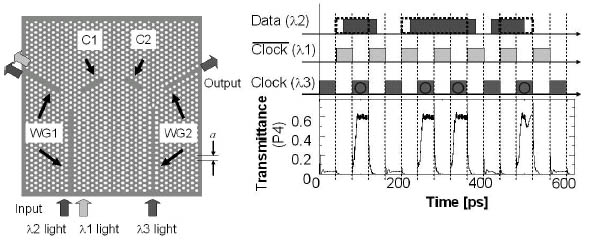
devices with dimensions of a few wavelengths of light. Figure 1 shows the
schematic structure of our flip-flop circuit based on a 2D-PhC with a triangular
air-hole lattice [1]. The lattice constant a is 400 nm, and the air-hole
diameter is 0.55a. The two resonators (C1, C2) have one identical resonant
wavelength (É…2) and two different resonant wavelengths (É…1 and É…3 for
C1 and C2, respectively). The waveguides (WG1, WG2) are tuned so that the
É…1 and É…3 lights can propagate in both WG1 and WG2, and the É…2 light
can propagate only in WG1.
Å@Here, we consider a situation where the input data (DATA: É…2 = 1548
nm) with a non-return-to-zero (NRZ) format deviates from the internal system
clock. In order to synchronize the data and the clock, we set all the input
powers of the É…1, É…2 and É…3 lights at 60 mW to employ the bistable operation
of C1 and C2, and used two signals as internal system clocks (CLOCK:É…3
= 1463 nm, CLOCK:É…1 = 1493 nm). We simulated our system with the 2D-FDTD
method taking account of the Kerr effect of the PhC material (AlGaAs).
Å@Figure 2 shows the calculated time charts of our system. This figure shows that our system outputs the AND signal between the ideal DATA (dotted line) and the CLOCK. That is, this system can synchronize the DATA with the CLOCK and regenerate the ideal DATA with a return-to-zero format. The system response time is about 10 ps, which means our system can operate with a 50 GHz clock.
Å@The result is the first step towards all-optical digital processing.
[1] A. Shinya, S. Mitsugi, T. Tanabe, M. Notomi, I. Yokohama, H. Takara, and S. Kawanishi, Optics Express 14 (2006) 1230
 |
|||||
|
|
||||