ü@
Eiichi Kuramochi, Takasumi Tanabe, Akihiko Shinya and Masaya Notomi
Optical Science Laboratory
ü@An advantage of photonic crystal (PC) nanocavities is compatibility of
a high quality factor (Q) with an ultra-small mode volume (V) [1].. A higher Q has been demanded in order to enhance device performance [2,3] and decrease
the device insertion loss resulting from the reduction in transmittance
caused by cavity-waveguide coupling. Although intensive studies have raised
the theoretical Q value to 106 [1], a further increase will be difficult to achieve using conventional
approaches.
ü@A new scheme for realizing a higher Q PC nanocavity involves a Fabry-Perot cavity composed of a loss-less line-defect
mode and two mode-gap mirrors [4]. The use of a mode-gap mirror instead
of a photonic bandgap (PC) mirror greatly reduces the out-of-plane loss
from the cavity because of the smooth and gradual decay of the electromagnetic
field in the mode-gap barrier region. We have found that such a mode-gap
can be generated by modulating the line-defect width [1]. In this study,
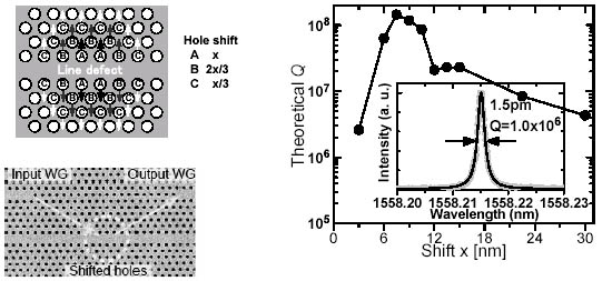
we designed a nanocavity in which holes around the cavity center were shifted
away from a line defect. In addition, we employed a tapered shift structure
(this 3-stage structure is shown in Fig. 1) in which a gradual change of
line-defect width enhanced the advantage of the mode-gap mirror. Numerical
studies with the 3D finite difference time domain method revealed that
the 3-stage structure can achieve an ultrahigh-Q (108) with an ultrasmall V (1.7 (ā╔/n)3 ). Next, we fabricated this structure in a Si PC slab by using electron
beam lithography [5]. The intensity spectrum of the cavity resonant mode
is shown in Fig. 2. The ultranarrow linewidth (1.5 pm) corresponded to
a Q of 1.0ü~106.
ü@In summary, our newly designed cavity has increased the theoretical Q value by two orders of magnitude and we achieved an experimental Q of one million for the first time as a PC-based nanocavity [6]. The Q achieved here is sufficiently high for many device applications and this
report is a first step towards adding new functions (optical buffering
and optical delay) to PC-based devices.
[1] M. Notomi et al., Opt. Express 12 (2004) 1551.
[2] M. Notomi et al., Opt. Express 13 (2005) 2678.
[3] T. Tanabe et al., Opt. Lett. 30 (2005) 2575.
[4] E. Kuramochi et al., Appl. Phys. Lett. 88 (2006) 041112.
[5] E. Kuramochi et al., Phys. Rev. B72 (2005) 161318(R).
[6] E. Kuramochi et al., LEOS2005, PD1.1 (2005).
 |
|||||
|
|
||||