Å@
Katsuhiko Nishiguchi, Yukinori Ono, and Akira Fujiwara
Physical Science Laboratory
Å@One class of memory device that could allow further shrinking of the MN is a gain-cell DRAM, in which a small signal originating from electrons stored in the MN is amplified by a nearby transistor. However, good scalability of the MN in the gain-cell DRAM raises another problem: a smaller MN means fewer electrons in the MN, which leads to shorter retention time. The dominant origin of this short retention is a current leakage originating from a p-n junction formed in the MN. A consequence of this problem is that the data-refresh process, i.e., periodic data read-out and storage, would have to be performed more frequently than in ordinary DRAMs, which would increase power consumption.
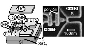
Å@We thus fabricated a log-data-retention gain-cell DRAM without p-n junction. The device is composed of two transistors, FET1 and FET2, which transfer and detect electrons, respectively. Both were fabricated on an undoped silicon-on-insulator (SOI) wafer (Fig. 1)[1]. The upper gate (UG) is used to induce an inversion layer in the undoped FET1 channel. When the lower gate (LG) turns FET1 off, an energy barrier under the LG electrically forms the MN at the tip of the wire channel of FET1. By opening and closing FET1, the data Åe0Åf and Åe1Åf are respectively represented by the presence and absence of electrons in the MN, which are introduced from the electron reservoir (ER). Then, the stored data, i.e. electrons, are read out as the change in current flowing through FET2, which is capacitively coupled to the MN.
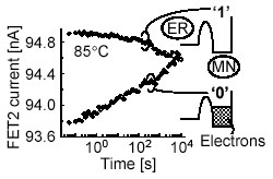
Å@Figure 2 shows that the fabricated device provides extremely long data retention (Å`104 s) even at 85 Åé. This is because the p-n junction formed at the boundary of the MN and FET1 in conventional DRAMs is replaced with the inversion layer formed by the UG, as shown in the insets of Fig. 2. Additionally, fast data storage (Å`10 ns) and dynamic random access comparable to those of conventional DRAMs were also confirmed.
Å@The demonstrated long data retention reduces the data-refresh cycles, thereby leading to low power consumption. The fabrication process is highly compatible with MOSFET circuits and is therefore promising for building gain-cell DRAMs embedded into logic circuits.
[1] K. Nishiguchi, et al., IEEE Electron Device Lett. 28 (2007) 48.
 |
 |
||||
|
|