Å@
Yukinori Ono, Katsuhiko Nishiguchi, and Akira Fujiwara
Physical Science Laboratory
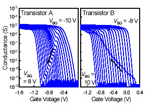
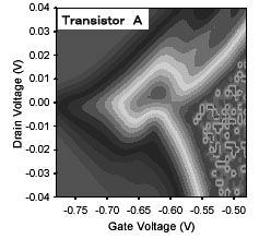
Å@Nano transistors whose gate length and width are both 40 nm were fabricated on a silicon-on-insulator substrate. The transistors comprise the channel lightly doped with boron, p-type source/drain, and electrically formed leads inserted between the channel and the source/drain. The insertion of the leads prevents the dopant diffusion from the source/drain and enables us to investigate the conductance of the channel containing only a few dopant atoms. The conductance was measured at 26 or 6 K as a function of the gate voltage using the substrate voltage (VBG) as a parameter. Figure 1 shows examples of the conductance characteristics for transistors with the doping density of 2Å~1016 cm-3, corresponding to the mean boron number in the channel of around one. The conductance modulation, indicated by the arrows, was observed in such lightly doped transistors but not in undoped ones. Figure 2 shows the differential conductance as functions of the gate and drain voltages, which demonstrates that the conductance modulation in Fig. 1 is due to the capture and emission of a single hole by and from a single boron acceptor.
Å@The conductance level of the modulation peak was strongly dependent upon VBG and the dependence was different from one transistor to another (Fig. 1), which is because of the random doping of boron atoms. This suggests that the VBG dependence conveys the information about the location (depth) of the boron and thus could lead to a way to count the dopant-atom number and measure the location of individual dopant atoms in a transistor.
[1] Y. Ono, et al., Jpn. J. Appl. Phys. 44 (2005) 2588.
[2] Y. Ono, et al., Phys. Rev. B 74 (2006) 235317.
[3] J.-F. Morizur, et al., Phys. Rev. Lett. 98 (2007) 166601.
[4] Y. Ono, et al., Appl. Phys. Lett. 90 (2007) 102106.
 |
 |
||||
|
|