Å@
Materials Science Laboratory
Å@Å@Diamond is expected to exhibit the best performance as an RF power
transistor because it has the highest breakdown field strength and thermal
conductivity and relatively high mobility and saturation velocity. Recently,
we have reported high RF performance in diamond FETs using H surface-termination
as p-type doping: cut-off frequencies of the current gain, fT (transition frequency), of 45 GHz and of the power gain, fMAX (maximum frequency of oscillation), of 120 GHz, and RF output power density
of 2.1 W/mm at 1 GHz in class-A operation. These values are the highest
among diamond at present and high enough for power amplifiers in wireless
base stations. However, the mechanism of H surface-termination in diamond
FETs is still controversial, and the band diagram of a diamond FET has
not been clarified yet.
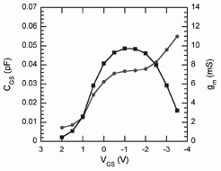
Å@Å@We have extracted the gate voltage dependence VGS of RF transconductance gm and gate-source capacitance CGS from S-parameter measurements of an FET with gate length (LG) of 0.1 mm and gate width (WG) of 50 mm, as shown in Fig. 1 [1]. The most significant finding is that
CGS shows a plateau for -0.5 V < VGS < -2.0 V. In the FET fabrication process, Al gate metal was deposited
directly on H-terminated diamond surface. However, this characteristic
unambiguously indicates that an energy barrier forms between the gate metal
and two-dimensional hole channel and that the diamond FET functions as
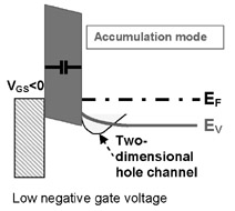
a MISFET. We have proposed the energy band diagram of the diamond FET,
as shown in Fig. 2.
Å@Å@As shown in Fig. 1, for VGS > -0.5 V, as positive VGS increases, gm decreases and CGS decreases. This means that as positive VGS increases, the depletion layer
below the energy barrier extends to the substrate side (Fig. 2). For VGS < -2.0 V, as negative VGS increases, gm decreases and at the same time CGS increases steeply. This characteristic indicates that the energy barrier
becomes a triangular potential barrier and then holes penetrate the energy
barrier, and consequently CGS increases. In Fig. 1, the CGS value at the plateau is 0.037 pF and its capacitance normalized by the
gate area is estimated to be 0.74 µF/cm2. Assuming the dielectric constant of diamond and Al2O3, the interfacial-layer thickness is estimated to be 7Å`10 nm. By cross-sectional
TEM observation, we have confirmed a 7Å`10 nm-thick interfacial layer between
Al gate metal and H-terminated diamond [2].
Å@Å@This work was partly supported by the SCOPE project, "Diamond
RF Power Amplifiers", from the Ministry of Internal Affairs and Communications,
Japan.
[1] M. Kasu, et al., Appl. Phys. Lett. 90 (2007) 043509.
[2] M. Kasu, et al., Diamond and Relat. Mater. 17 (2008) in press.
 |
 |
|||||
|
|