ü@
Materials Science Laboratory
ü@ü@GaN-based electronic devices are expected to be advantageous for high-power
and high-temperature operation compared with conventional GaAs- or Si-based
devices because of the wide band gap of GaN. In the previous studies, we
have succeeded in obtaining the high current gain of over 2000 [1] and
high-power characteristics of 270 kW/cm2 [2] for the npn-type GaN/InGaN double heterojunction bipolar transistors
(DHBTs). Our next target is to demonstrate the high-temperature operation
of these DHBTs. In this study, we investigated the temperature dependence
of the common-emitter current-voltage (I-V) characteristics of npn-type GaN/InGaN DHBTs [3].
ü@ü@GaN/InGaN DHBT structures were grown on SiC substrates using low-pressure
metal-organic vapor phase epitaxy. The sample structure consisted of a
40-nm-thick n-GaN emitter, a 100-nm-thick p-InGaN base, a 30-nm-thick graded InGaN layer, a 500-nm-thick n-GaN collector, a 1-µm-thick n-GaN sub-collector, and an AlN buffer layer. The In composition of p-InGaN base was 7%. The emitter size was 50ü~30 µm2.
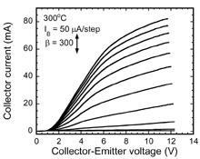
ü@ü@Figure 1 shows the common-emitter I-V characteristics of the GaN/InGaN DHBT measured at 300 üÄ. The base current
is 50 µA/step. Even though the current gain (ā└=āóIC/āóIB) decreases with increasing temperature, the maximum current gain at 300
üÄ is still as high as 308. The maximum current density at 300 üÄ is calculated
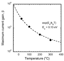
to be as high as 5.5 kA/cm2. As shown in Fig. 2, the temperature dependence of the maximum current
gain of the GaN/InGaN DHBT follows an exponential dependence with activation
energy of 0.13 eV. Since the activation energy of the reduction of the
current gain is larger than the expected value assuming the increase in
the hole back-injection current from the base into the emitter (0.06 eV),
an increase in the carrier concentration of the p-In0.07Ga0.93N base, which activation energy is 0.12 eV, is considered to be attributed
to the reduction of the current gain.
[1] T. Makimoto, K. Kumakura, and N. Kobayashi, Appl. Phys. Lett. 83 (2003) 1035.
[2] T. Makimoto, Y. Yamauchi, and K. Kumakura, Appl. Phys. Lett. 83 (2004) 1964.
[3] A. Nishikawa, K. Kumakura, and T. Makimoto, Appl. Phys. Lett. 91 (2007) 133514.
 |
 |
|||||
|
|