Å@
Materials Science Laboratory
Å@Å@Optical and electrical properties of nanostructures can be addressed
using radiation or electrical current as a probe. In general, a near-field
type of electromagnetic interaction is necessary for an optical probe to
enter nanoscale regime in the spatial resolution domain by overcoming the
optical diffraction limit (Å` 1 µm). A typical scanning near-field
optical microscope (aperture-SNOM) provides such an opportunity both for
the excitation and collection of light for spectroscopy applications. However,
this instrument utilizes a dielectric fiber tip as an aperture, which makes
it unsuitable for electrical measurements. On the other hand, a scanning
tunneling microscope (STM), capable of atomic-resolution measurements by
electrical current, can also cause luminescence of materials. Here, in
order to realize both electrical and optical probing at nanoscale, we combine
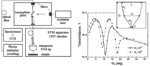
these two kinds of instruments into a single unit (Fig. 1).
Å@Å@In order to evaluate tip geometry influence on its performance for
various operation regimes finite element method (FEM) simulations were
carried out. It was found that tip transmittance for SNOM excitation mode
depends strongly on tip geometry away from the edge. A variation of nearly
two orders of magnitude is a result of constructive/destructive interference
of the excitation light (Fig. 2). Furthermore, the role of the opening
in protective metal film in light collection efficiency was simulated for
the STM-luminescence mode. Based on the present simulations one can choose
a suitable tip configuration from the interplay between the instrument
collection efficiency and its spatial resolution [1].
Å@Å@We aim at concurrent optical and electrical characterization of nanostructures
(e.g. quantum wells, dots, etc.) with high spatial resolution. In addition,
this approach may find its niche where electrical modification with subsequent
in situ optical probing is desirable.
[1] I. Sychugov, H. Omi, T. Murashita, and Y. Kobayashi, Appl. Surf. Sci., in press.
 |
|||||
|