Å@
1Materials Science Laboratory, 2Physical Science Laboratory
Å@Å@Recently, graphene has attracted much attention as a material for future
electronics [1]. So far, electronic device properties have been investigated
for graphene layers produced in two ways: graphene flakes exfoliated from
bulk graphite [1] and epitaxial graphene grown on SiC substrates by annealing
[2]. Epitaxial graphene grows on a wafer scale and is promising for device
integration. To make epitaxial graphene applicable, however, we need to
grow wide epitaxial graphene with the intended number of layers. As a base
of this growth control, we have established a way of determining the number
of graphene layers microscopically [3].
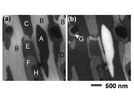
Å@Å@We evaluated the number-of-layers distribution in epitaxial graphene
grown on SiC by low-energy electron microscopy (LEEM) using quantized oscillations
of electron reflectivity. Figure 1 shows LEEM images of epitaxial graphene
on 4H-SiC(0001) at various electron beam energies, which corresponds to
the mappings of the secular electron reflectivity in the normal incidence.
These images show that the electron reflectivities in different regions
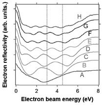
change with the energy in different manners. Figure 2 shows the energy
dependence of the electron reflectivities in areas A-H. The reflectivity
oscillates with the electron beam energy.
Å@Å@Bulk graphite has continuous electronic bands normal to the graphene
sheet, but these bands split into discrete energy levels in graphene layers
due to their finite thickness. When the energy of incident electrons coincides
with one of the discrete energy levels, the electrons resonantly transmit
through the layers, resulting in dips in the reflectivity. Therefore, the
number of graphene layers can be counted directly as the number of dips
in the reflectivity. The validity of this scenario was confirmed by the
result that the quantized conduction band states calculated using tight-binding
and first-principles methods well reproduce the dip positions in the reflectivity.
In-situ microscopic determination of the number of graphene layers using LEEM
would greatly contribute to the growth control of epitaxial graphene.
Å@Å@This work was partly supported by KAKENHI (19310085) from the Ministry
of Education, Culture, Sports, Science and Technology of Japan.
[1] K. S. Novoselov and A. K. Geim, Nature Materials 6 (2007) 184.
[2] C. Berger, et al., Science 312 (2006) 1191.
[3] H. Hibino, et al., Phys. Rev. B 77 (2008) 075413; H. Hibino, et al., e-J Surf. Sci. Nanotechnol. 6 (2008) 107.
 |
 |
|||||
|
|