Å@
Physical Science Laboratory
Å@Å@Continuously growing information technology markets have been expanding
the application fields of sensor devices. Among the various kinds of sensors,
Si-based image sensors using charge-coupled devices, photo diodes, and
so on, have been used extensively because of their highly useful features,
such as high miniaturization and integration, compared to those made of
other materials. A basic mechanism of these sensors is that photons with
visible wavelengths, whose energy is larger than the band gap of Si, generate
electron-hole pairs. Whereas an infrared (IR) signal with wavelength longer
than the visible one is useful for numerous applications, such as remote
sensing, thermal sensing, and material analysis, a Si-based IR sensor is
not good at detecting IR signal, compared to other sensors, because it
does not have enough energy for electron-hole pairs to be generated.
Å@Å@We thus developed a new method of detecting an IR signal using a Si-based
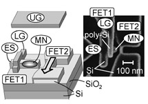
device [1]. The device is composed of two transistors fabricated on a silicon-on-insulator
wafer (Fig. 1). The first transistor (FET1) has a two-layer gate: an upper
gate (UG) is used to induce an inversion layer and a lower gate (LG) forms
an energy barrier in the undoped channel of FET1. As a result, an electron-storage
node (MN) electrically isolated from an electron source (ES) is formed.
IR irradiation to FET1 excites electrons in the ES and some of the excited
electrons diffuse into the MN over the energy barrier formed by the LG.
The tiny charge originating from electrons in the MN are detected with
high charge sensitivity by the other transistor (FET2), whose channel is
capacitively coupled to the MN.
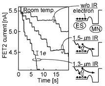
Å@Å@Figure 2 shows the change in FET2 current with and without IR radiation.
The FET2 current decreased stepwise with the same height, which means that
one electron, which entered the MN from the ES, was detected as one step
of the FET2 current owing to the high charge sensitivity of FET2. The increase
in electron injection into the MN by IR radiation means that electrons
in the ES were excited and then injected into the MN over the energy barrier
under the LG, which enables a function of IR-signal detection. An IR signal
with shorter wavelength caused more frequent electron injection into the
MN. This enables the device to function as a short-wave length pass filter
by controlling the energy barrier using the LG. Additionally, since the
number of electrons excited by an IR signal is proportional to electron
density in the ES, which is controlled by the UG, IR signal sensitivity
can be controlled by the UG. Since the demonstrated Si-based device can
detect an IR signal with new functions electrically controlled by gates,
its applications could be expanded to various fields.
[1] K. Nishiguchi, et al., Appl. Phys. Lett. 90 (2007) 223108.
 |
 |
|||||
|
|