Å@
Physical Science Laboratory
Å@Å@Clocked transfer of single electrons is attracting a great deal of
interest in its application to current standards in metrology and integrated
single-electron (SE) circuits. While the conventional metal-based SE pumps
and turnstiles employ fixed tunnel junctions of metal oxide, the use of
gate-induced electrostatic tunable barriers in semiconductors has a clear
advantage for higher-frequency operation because the tunnel resistance
can be tuned to reduce the RC time. Although we showed 100-MHz operation
of an SE turnstile using Si nanowire MOSFETs with two barriers modulated
by two phase-shifted AC signals [1], higher-frequency operation is desired
because nanoampere current is necessary for the so called metrological
triangle experiment.
Å@Å@We recently developed a nanoampere SE pump operated based on a simple
scheme using only one AC signal applied to one gate [2]. We named the proposed
device an SE ratchet since it utilizes the asymmetry potential to capture
electrons from the source and eject them to the drain, thereby causing
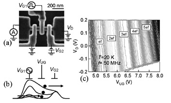
directional SE transport without any source-drain bias. Figures 1(a) and
1(b) show a top-view scanning-electron-microscope (SEM) image of the device
and a schematic diagram of the ratchet potential, respectively. We apply
AC pulse voltage VG1 at frequency f to the center gate and constant lower voltage VG2 to the drain-side gate. SEs are captured from the source into the island,
and then ejected to the drain. The number of transferred electrons per
cycle is controlled by the upper gate voltage, VUG. As shown in Fig. 1 (c), current plateaus (I = mef, m: integer) are clearly observed at 20 K in a wide range of the drain bias
(VD), which indicates that the SE transfer is directional regardless of the
bias polarity. The VD range can be much larger than the charging energy of the island (Å`10
meV) thanks to the potential control of the island as well as the barrier.
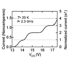
Nanoampere charge pumping is obtained at f =2.3 GHz as shown in Fig. 2. The transfer accuracy is roughly estimated
to be in the order of 10-2. It is found that the nonadiabacity of the electron capture affects the
shape of the current steps. This is an important finding for further study
towards higher accuracy. The SE ratchet is a promising device in the application
to large-current source for metrological standards. This work was partially
supported by KAKENHI (16206038, 19310093).
[1] A. Fujiwara, et al., Appl. Phys. Lett. 84 (2004) 1323.
[2] A. Fujiwara, et al., Appl. Phys. Lett. 92 (2008) 042102.
 |
 |
|||||||||
|
|