Materials Science Laboratory
Ion implantation is a widely used doping technique for Si and GaAs. However,
in the case of diamond, implantation-induced damage cannot be recovered
by conventional thermal annealing because its annealing condition is not
located in diamond stable phase but in graphite stable phase. Previously,
we reported that high pressure and high-temperature (HPHT) annealing in
diamond stable phase is highly effective to recover damages induced during
ion-implantation [1]. In this study, we achieved higher hole concentration
and mobility using this technique and successfully fabricated diamond FETs
[2].
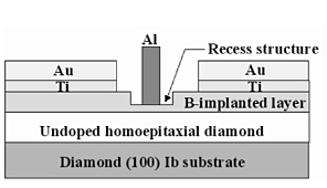
CVD homoepitaxial diamond films were grown on Ib (100) substrates by microwave
plasma CVD. Then, boron (B) ions were implanted in the films at an acceleration
energy of 60 keV with a dose of 1015〜1016 cm-2. HPHT annealing of the B-implanted films was performed at 〜7 GPa and 1350ºC
for activation of dopants. Using these diamond films, FETs were fabricated
(Fig. 1). The source and drain contacts were formed by Ti/Au with annealing
at 600ºC. The Schottky-gate contact was formed by the evaporation
of Al.
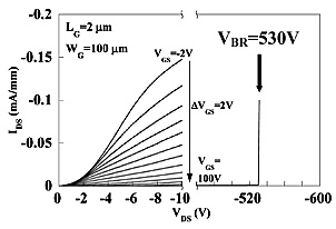
We obtained a higher hole concentration for a dose of 1〜5×1015 cm-2 while keeping high mobility. For a dose of 3×1015 cm-2, we obtained sheet concentration and mobility at 300 K of 1.6×1013 cm-2 and 41 cm2/Vs, respectively. These values are comparable to those of H-terminated
diamond (〜1013 cm-2 and 〜100 cm2/Vs) widely used so far. Using this film with a dose of 3×1015 cm-2, we fabricated FETs. The gate length and the width were 2 µm and
100 µm, respectively. Current saturation and pinch-off characteristics
were clearly observed. The maximum IDS of 0.15 mA/mm was obtained at VGS of -2 V (Fig. 2). The forward breakdown voltage (VBR) of the FET was 530 V. Breakdown of the point was destructive and part
of Al Schottky and Au/Ti ohmic electrodes melted. The breakdown electric
field was estimated to be 〜1.1 MV/cm. The Ec is comparable to those of Al-Schottky diodes using B-doped CVD homoepitaxial
diamond films [1, 2]. The result also indicates the high quality of our
B-implanted layers.
This work was partly supported by the SCOPE project of the Ministry of
Internal Affairs and Communications, Japan.
[1] K. Ueda, M. Kasu, and T. Makimoto, Appl. Phys. Lett. 90 (2007) 122102.
[2] K. Ueda and M. Kasu, Physica Status Solidi (c) 5 (2008) 3175.
 |
 |
|||||
|
|