Materials Science Laboratory
There are large mismatches between III-nitride semiconductors and conventionally
used sapphire substrates in terms of the lattice constant or thermal expansion
coefficient. Therefore, the most suitable substrate for GaN growth is no
doubt the GaN substrate. From the viewpoints of device applications, the
merits of using GaN substrates are as follows: a low dislocation of the
substrate itself, resulting in improving the device performance, or a relatively
large thermal conductivity, making it possible to spread heat generated
under a high-power operation. In principle, heterojunction bipolar transistors
(HBTs) have the ability to operate with uniform threshold voltages and
high current densities. A normally off characteristic is advantageous for
a fail-safe system. Therefore, nitride-based HBTs are one of the attractive
devices for high-power electronics. In this work, we fabricated the pnp AlGaN/GaN HBTs on GaN substrates and showed their high performance at
room temperature (RT).
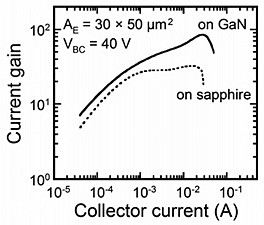
Figure 1 shows current gains as a function of the collector current (Ic) of pnp AlGaN/GaN HBTs on sapphire and GaN substrates measured at RT. The HBTs
on GaN substrates exhibited a high performance: a maximum current gain
of 85 at a collector current of 30 mA and a maximum collector current density
of 7.3 kA/cm2 at a collector-emitter voltage of 30 V, which corresponds to the maximum
power dissipation density of 219 kW/cm2. The current gain and the collector current density increased compared to those on sapphire substrates. The calculated minority carrier diffusion length agreed well with that determined from electron beam induced current measurements [1]. Therefore, these results indicate that the current gain was dominated by the minority hole diffusion in the neutral base at high Ic for the HBTs on the GaN substrates, and that the increase in the current
gain is ascribed to the low dislocation density in the HBTs. For the HBT
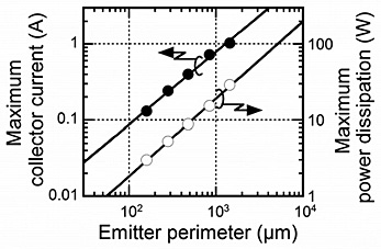
with the large emitter area, the current gain was still as high as 47 and
the maximum collector current reached as high as 1 A, and this single HBT
showed a high-power dissipation of 30 W as shown in Fig. 2. This high performance
of the HBTs is ascribed to the low dislocation density and relatively high
thermal conductivity of the GaN substrate.
[1] K. Kumakura et al., Appl. Phys. Lett. 86 (2005) 052105
 |
 |
|||||
|
|