Materials Science Laboratory
Hexagonal boron nitride (h-BN), with its wide bandgap in the deep ultraviolet region, has been gaining
interest since it was proposed as a promising material for optoelectronic
applications. The h-BN epitaxial growth has been achieved using the metalorganic vapor phase
epitaxy (MOVPE) [1]. Parasitic reactions between sources in BN epitaxy
by MOVPE can be avoided in molecular beam epitaxy (MBE) growth of h-BN. However, a polycrystalline BN structure was obtained by MBE and no
successful MBE-grown h-BN epitaxy has been reported yet.
Here, we report the epitaxial h-BN growth on Ni(111) substrate by MBE [2]. Elemental boron evaporated
by an electron-beam gun and active nitrogen generated by a radio-frequency
(RF) plasma source were used as the group-III and -V sources, respectively.
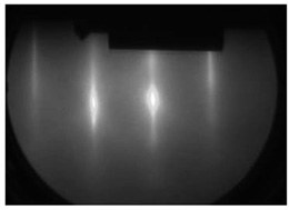
Figure 1 shows in-situ reflection high energy electron diffraction (RHEED)
pattern taken along the [
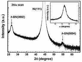
A representative XRD for the 1000 Å h-BN epitaxial film is shown in Fig. 2. Diffraction peaks from both the
h-BN(0002) and h-BN(0004) planes along with the underlying Ni(111) substrate prove the
formation h-BN with the orientation of h-BN[0001] parallel to the Ni[111] direction. The inset of Fig. 2 shows the x-ray rocking curve of the h-BN epitaxial film characterized by the full width at half maximum (FWHM)
of 0.61º. This FWHM from a 1000 A film is narrower than the best value
ever reported [1], and can possibly be further decreased by optimizing
the growth conditions and/or increasing the epitaxial film thickness. From
the RHEED observation and XRD, the alignments between the h-BN film and the Ni substrate are [0001]h-BN || [111]Ni, [11
[1] Y. Kobayashi et al., J. Crystal Growth 298 (2007) 325.
[2] C.L. Tsai et al., J. Crystal Growth (in press).
 |
 |
|||||
|
|