Materials Science Laboratory
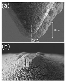
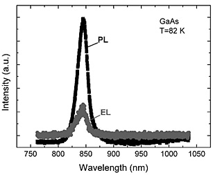
Optical and electrical properties of nanostructures can be addressed using electromagnetic radiation or electrical current as a probe. In general, a near-field type of electromagnetic interaction is necessary for an optical probe to enter nanoscale regime in spatial resolution by overcoming the optical diffraction limit (〜1 µm). A typical aperture scanning near-field optical microscope (aperture-SNOM) provides such an opportunity both for the excitation and collection of light. However, this instrument employs a dielectric fiber tip as an aperture, which makes it unsuitable for electrical measurements. An apertureless SNOM, on the contrary, has a metallic, needle-like opaque tip. The local field enhancement at the tip apex due to the plasmon effect enhances signal in the light scattering experiments. But, unlike the case of aperture-SNOM, the far-field optics alignment is necessary and the scattered light from the tip shaft can distort the measurements. In addition, the aperture-SNOM can operate in the combination with a scanning tunnelling microscope (STM) and it was demonstrated that such a combination can yield superior resolution for SNOM imaging compared to the conventional shear-force approaching method. On the other hand, the STM, which is capable of atomic-resolution measurements using electrical current, can also cause an optical response in materials. The collection of light in ordinary STM machines with opaque metal tips is realized by far-field optics. When the carriers are tunnelled to the sample it is the excitation (tunnelling) area that limits the spatial resolution; the achieved resolution of such an instrument was reported to be as small as 〜10 nm. The collection efficiency of the emitted light can be improved by employing a transparent STM tip, where the light is coupled directly to the tip rather than to a far-field detector. However, only the electrical probing of nanostructures was proven feasible in such a scanning tunnelling microscope luminescence (STML) experiment. We expand the STML approach to show an ultimate STM-based configuration with the aperture metal tip (Fig. 1), where both optical and electrical excitations are available (Fig. 2). This method enabled us to characterize the same area in near-field of the sample through the aperture of transparent tip covered with metals [1].
[1] I. Sychugov, H. Omi, T. Murashita, and Y. Kobayashi, Nanotechnology 20 (2009) 145706.
 |
 |
|||||
|
|