Physical Science Laboratory
Although the miniaturization of Si metal-oxide-semiconductor field-effect
transistors (MOSFETs) continues to improve the performance of various consumer
electronics, the need to guarantee error-free operation of MOSFETs makes
it difficult to reduce supply voltage, which leads to ever increasing current
density and power consumption. In this work, conversely, we reduce the
current density of nanoscale FETs ultimately and then utilize its shot
noise to realize a stochastic data processing for pattern recognition with
high flexibility [1].
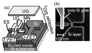
The device is composed of two transistors fabricated on a silicon-on-insulator
wafer (Fig. 1). The first transistor (T-FET) has a two-layer gate: an upper
gate (UG) is used to induce an inversion layer and a lower gate (LG) forms
an energy barrier in the undoped channel of T-FET. As a result, an electron-storage
node (MN) electrically isolated from an electron source (ES) is formed.
The two layer gate can eliminate undesired leakage current originating
from p-n junctions, which is a well-known issue in conventional FETs [1, 2]. Therefore,
highly controllable single-electron transfer from the ES to the MN can
be achieved using the LG. The single electrons transferred to the MN are
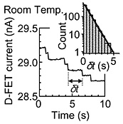
detected by the other transistor (D-FET) as shown in Fig. 2. The optimization
of the device structure and operation conditions allows single-electron
detection even at room temperature [3]. As analysis of the time interval
δt of each electron transfer to the MN revealed that the single-electron
transfer is based on a Poissonian process (inset of Fig. 2), which corresponds
to the real-time monitoring of shot noise in FETs with single-electron
resolution.
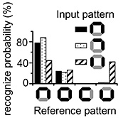
The Poissonian stochastic behavior of such single-electron transfer can be applied to a stochastic data-processing circuit for image-pattern recognition. The circuit recognizes the input pattern as one of the reference patterns with probability correlating to the similarity between the reference and input patterns as shown in Fig. 3. Such probability can be electrically controlled by the LG. These features allow flexible pattern recognition especially for corrupted input patterns, which promises to apply high time and power efficiency to the circuit like in the human brain.
[1] K. Nishiguchi et al., Appl. Phys. Lett. 92 (2008) 062105.
[2] K. Nishiguchi et al., IEEE Electron Device Lett. 28 (2007) 48.
[3] K. Nishiguchi et al., Jpn. J. Appl. Phys. 47 (2008) 8305.
 |
 |
 |
||||||||
|
|
|