Physical Science Laboratory
Electron-hole bilayers in which a two-dimensional electron gas (2DEG)
and a two-dimensional hole gas (2DHG) coexist in close proximity have received
considerable interest owing to the possibility of their hosting a condensation
of indirect dipolar excitons [1]. Here, we examine the low temperature
transport properties of a device in which electrons and holes are simultaneously
generated but separately contacted [2] in a 40 nm thick layer of silicon.
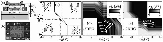
The device consists of a Silicon-On-Insulator transistor [Fig. 1(a)] in
which the front- and back-gates allow sufficient electric field in the
silicon quantum well to overcome the band-gap so that a 2DEG and 2DHG can
be generated simultaneously at opposite sides of the well. The device is
cut into a Hall-bar where each of the arms is terminated by p- and n-type contacts [Fig. 1(b)] made by ion implantation of B and P respectively
[3]. The n-contacts (p-contacts) connect to the 2DEG (2DHG) but the p-contacts (n-contacts) do not due to the depletion regions formed at each junction between the 2DEG (2DHG) and the p-contacts (n-contacts) leading to independent contacts.
Low temperature measurements of Shubnikov de Haas oscillations [Fig. 1(d)
and Fig. 1(e)] show that the charge carriers are generated at the expected
positions in the structure [Fig. 1(c)] and that their densities can be
controlled by an interlayer bias applied between the 2DEG and 2DHG in addition
to the gate voltages. This allows the electric field (confinement potential)
to be tuned in the quantum well, and in turn allows the physical properties
of the carriers such as the strength of disorder and electronic valley
splitting to be controlled [4]. We confirm that drag measurements are possible
with the structure [5]. We expect that the structure will allow many new
measurements to probe the physics of electron-hole systems.
[1] Y. E. Lozovik and V. I. Yudson, JETP Lett. 22 (1975) 556.
[2] U. Sivan, P. M. Solomon, and H. Shtrikman, Phys. Rev. Lett. 68 (1992) 1196.
[3] K. Takashina et al., Extended Abstracts of the 2006 International Conference
on Solid State Devices and Materials, Yokohama 2006, pp.830-831; K. Takashina
et al., Jpn. J. Appl. Phys. 46 (2007) 2596; M. Prunnila et al., Appl. Phys. Lett. 93 (2008) 112113.
[4] K. Takashina et al., Phys. Rev. Lett. 96 (2006) 236801.
[5] K. Takashina et al., Appl. Phys. Lett. 94 (2009) 142104.
 |
||
|