 |
| Photograph of atomic force microscopy |
|
| Photograph of atomic force microscopy |
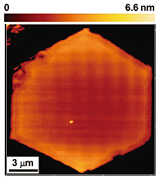
Step-free GaN Surfaces Fabricated by Selective-area Metalorganic Vapor Phase Epitaxy A step-free GaN surface with the diameter of 16 µm, which was atomically flat without any monolayer steps, was fabricated for the first time by selective area metalorganic vapor phase epitaxy. This technique can control the hetero-interfaces of nitride semiconductors in an atomic scale and realize high-efficiency light emitting devices and sabband devices, such as resonant tunneling diodes and cascade lasers. In addition, we clearly observed the nucleus growth of nitride semiconductors and investigate the mechanism in detail. (Page 16)
[back] [Top] [Next]