Materials Science Laboratory
Step-free surfaces of GaN-related nitride semiconductors have been strongly desired for studying growth mechanisms and for achieving the abrupt hetero-interfaces necessary for nitride-based devices, such as laser diodes, resonant tunneling diodes, and cascade lasers. Previously reported surfaces of nitride semiconductors, however, showed a high density of monolayer steps originating from crystal defects (dislocations). Here, we report the first successful fabrication of step-free GaN surfaces, which are covered with single wide atomic terraces without any monolayer steps. The step-free surfaces were obtained by using GaN substrates with low dislocation densities and by optimizing growth conditions, such as temperature, growth rates, and the V/III ratio [1].
First, a SiO2 mask was deposited on a GaN (0001) substrate with low dislocation density (~106 cm-2). Then, the SiO2 mask was patterned by photolithography so as to have many hexagonal openings
with the diameter of 16 µm. Finally, selective-area metalorganic
vapor phase epitaxy (SA-MOVPE) of GaN films was performed onto the mask-patterned
GaN substrate. Source gases were ammonia and trimethylgallium (TMG).
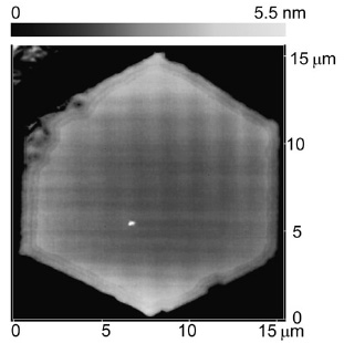
Figure 1 shows an atomic force microscopy (AFM) image of a GaN surface fabricated at 940ºC and at the TMG flow rate of 2.6×10⁻⁵ mol/min. The surface has a single wide terrace over almost its whole area
(step-free surface) except at the edges and there are no screw-type dislocations
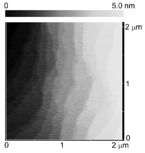
within the GaN hexagon. On the other hand, a GaN surface fabricated by
conventional MOVPE exhibited a high density of monolayer steps with an
average interstep distance of ~0.1 µm (Fig. 2). In addition, a GaN surface fabricated by SA-MOVPE
under non-optimized growth conditions had several ten monolayer steps.
In conclusion, we fabricated step-free GaN surfaces with the diameter
of 16 µm by SA-MOVPE using GaN substrates with low dislocation density
under optimized conditions.
[1] T. Akasaka, Y. Kobayashi, and M. Kasu, Appl. Phys. Express 2 (2009) 091002.
 |
 |
|||||
|
|