1Materials Science Laboratory, 2Kyushu University, and 3Physical Science Laboratory
Few-layer graphene (FLG) is attracting intense attention as a future electronics
material due to its superior electronic transport properties. Epitaxial
FLG grown on SiC substrates by thermal decomposition can be easily scaled
up and is promising for device integration. We have so far established
a method of determining the number of graphene layers microscopically using
low-energy electron microscopy (LEEM) [1] and have succeeded in growing
bilayer graphene a few micrometers in size. In this work, we clarified
the domain structures in bilayer graphene [2].
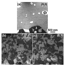
Figure 1 shows LEEM images of FLG 1-3 layers thick grown on 4H-SiC(0001).
Bilayer graphene looks continuous in the bright-field LEEM image [Fig.
1(a)] obtained using the specularly reflected (0,0) beam. However, the
dark-field LEEM images [Figs. 1(b) and 1(c)] obtained using the diffracted
(1,0) and (0,1) beams clearly show that bilayer graphene contains two types
of domains. The contrast of the two domains are reversed between the (1,0)
and (0,1) dark-field LEEM images, indicating that these domains have three-fold
symmetry. Monolayer graphene has six-fold symmetry, and two carbon atoms
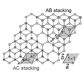
are located at A and B sites in a unit cell. On the other hand, as shown
in Fig. 2, bilayer graphene can have two types of stacking orders with
three-fold symmetry: AB stacking in which a B’ carbon atom is on an A carbon
atom and BA (usually called AC) stacking in which an A’ carbon atom is
on a B carbon atom. Therefore, we speculate that the two types of domains
seen experimentally correspond to the AB and AC stackings. To confirm this,
we measured the energy dependence of the intensities of the dark-field
LEEM images for the two domains and compared it to the calculated energy
dependence of the (1,0) and (0,1) low-energy electron diffraction intensities
for bulk graphite. Good agreement between these two energy dependences
proves that there are stacking domains in bilayer graphene. The stacking
domain structures can affect the electronic transport properties in FLG.
The formation mechanism and condition for growing a single stacking domain
are the next targets.
This work was supported by KAKENHI.
[1] H. Hibino et al., Phys. Rev. B 77 (2008) 075413.
[2] H. Hibino et al., Phys. Rev. B 80 (2009) 085406.
 |
 |
|||||
|
|