Physical Science Laboratory
Block copolymer lithography has drawn considerable attention as a combined
top-down/bottom-up nanopatterning method toward 16-nm-technology nodes
and beyond. The most important challenge of its application to nanodevice
fabrication is in achieving two-dimensional (2D) patterning by strictly
controlling the alignment of the domain interface of the microphase-separated
domains of a block copolymer. Here, we demonstrated that a flexibly designable
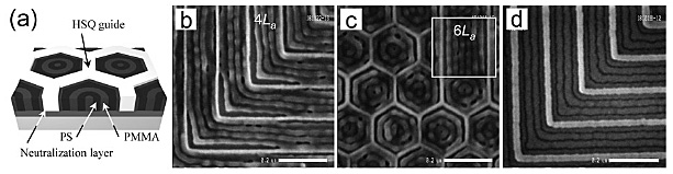
2D self-assembly of the symmetric poly(styrene-b-methylmethacrylate) (PS-b-PMMA) (Mn: 36 kg mol-1, lamellar period L0=28 nm) is achieved by graphoepitaxy using a hydrogen silsesquioxane (HSQ) resist pattern as the guide for alignment [1]. The key to success is the combination of the neutralization of the bottom surface and the introduction of an intentionally designed 2D hydrophilic guiding pattern formed by top-down electron-beam lithography (EBL), which leads to vertical orientation and 2D alignment of lamellar domains, respectively [Fig. 1(a)].
For rectangular confinement, vertical lamellar domains with a thickness
of 4La (La: average repeating period of the laterally aligned lamellar domains) and
with a half-pitch of 16 nm can be forced to bend using right-angled guiding
patterns [Fig. 1(b)]. It is noteworthy that these domain structures are
formed in a pure block copolymer system, which can be achieved with high
flexibility in the domain shape and period in graphoepitaxy of lamellar
domains of diblock copolymers. For hexagonal confinement, we have successfully
demonstrated that concentric cylindrical domains are formed [Fig. 1(c)];
these domains are characterized by high controllability of the number of
layers of the PS or PMMA rings, which is achieved by varying the width
of confinement between opposite sides. This precise control of the alignment
of lamellar domains can be achieved by first taking full advantage of the
bottom-up self-assembly of block copolymers and the top-down fabrication
of the alignment guide by using high-precision EBL. We have also confirmed
that these bent lamellae and concentric cylinders were successfully transferred
to a semiconductor substrate with a 16-nm half-pitch resolution [Fig. 1(d)].
We are convinced that our method increases the applicability of block copolymer
lithography to nanodevice fabrication, as the size scale is beyond the
reach of the state-of-art top-down technology.
[1] T. Yamaguchi and H. Yamaguchi, Adv. Mater. 20 (2008) 1684.
 |
||
|